Nonvolatile memory device and driving method thereof

a nonvolatile memory and driving method technology, applied in the direction of static storage, digital storage, instruments, etc., can solve the problems of increasing stress, high integration, and difficult for the typical nonvolatile memory device to have an optimized programming time, so as to achieve the effect of optimizing performan

Active Publication Date: 2008-08-28
SAMSUNG ELECTRONICS CO LTD
View PDF1 Cites 51 Cited by
  • Summary
  • Abstract
  • Description
  • Claims
  • Application Information

AI Technical Summary

Benefits of technology

[0015]Embodiments of the invention provide a nonvolatile memory device and method that optimize performance based on differences in threshold voltage distribution.

Problems solved by technology

In general, the NOR flash memory device is advantageous in high-speed performance, whereas it is disadvantageous in high integration due to its high current consumption.
Consequently, it is difficult for the typical nonvolatile memory device to have an optimized programming time because the program operating conditions are determined from the total threshold voltage distribution.
This leads to an increase in stress of a memory cell, resulting in deterioration of reliability of the memory cell in the long run.
That is, the typical nonvolatile memory device cannot optimize a sensing time.
However, the precharge time Tpc is limited by the precharge time of the odd-bitline BLo.
In this case, however, a cell current development time Td is limited by the development time of the even-numbered bitline BLe.
This leads to degradation in read / verify characteristics of a nonvolatile memory device.

Method used


Image

  • Nonvolatile memory device and driving method thereof
  • Nonvolatile memory device and driving method thereof
  • Nonvolatile memory device and driving method thereof

Examples


first embodiment

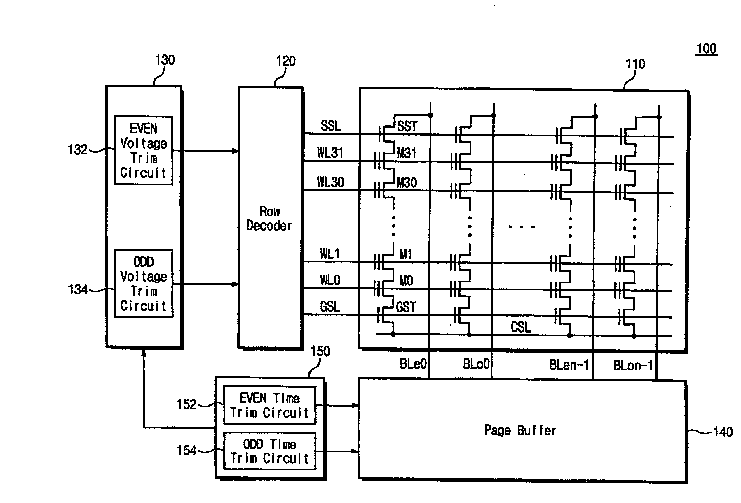
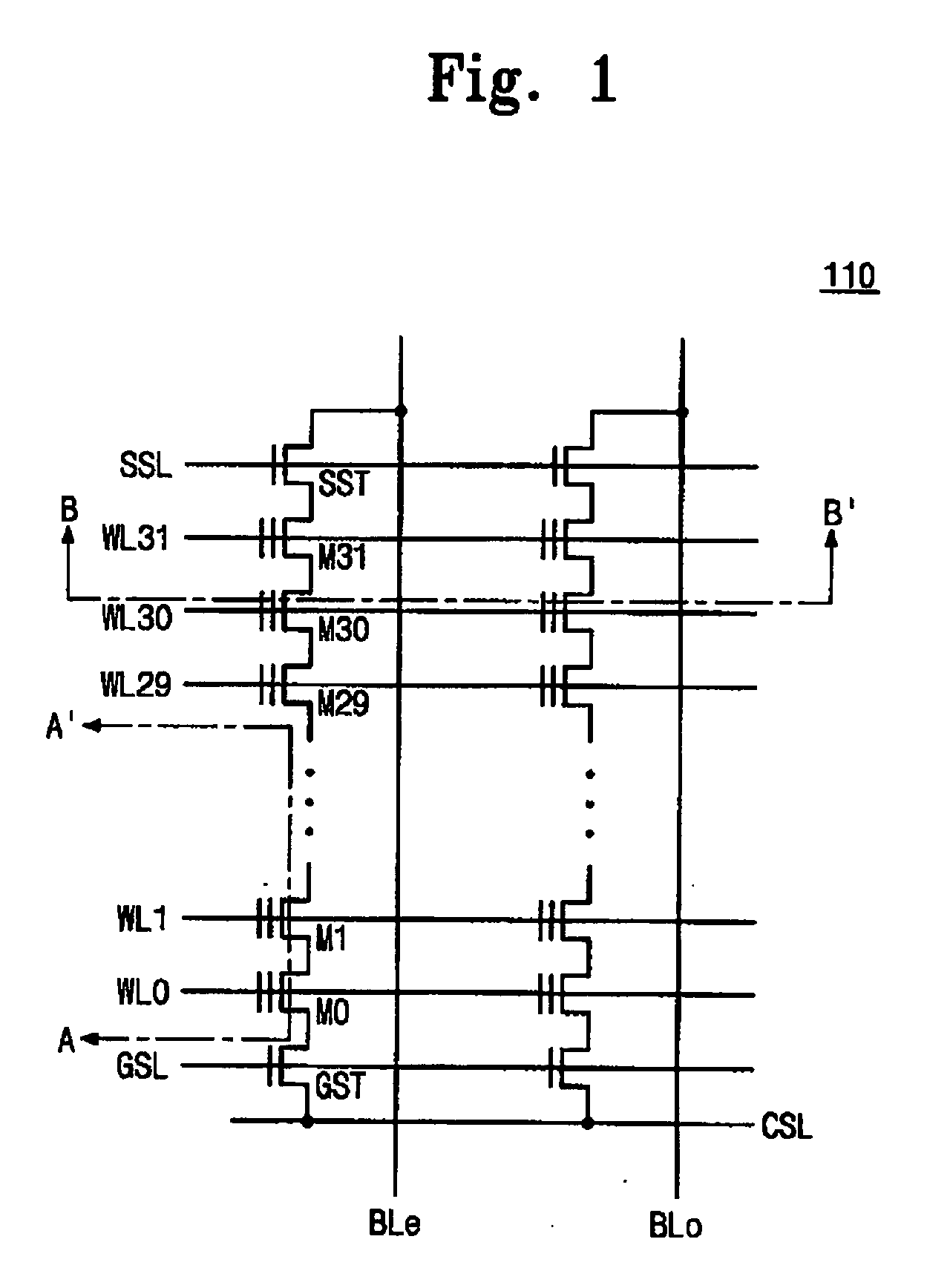
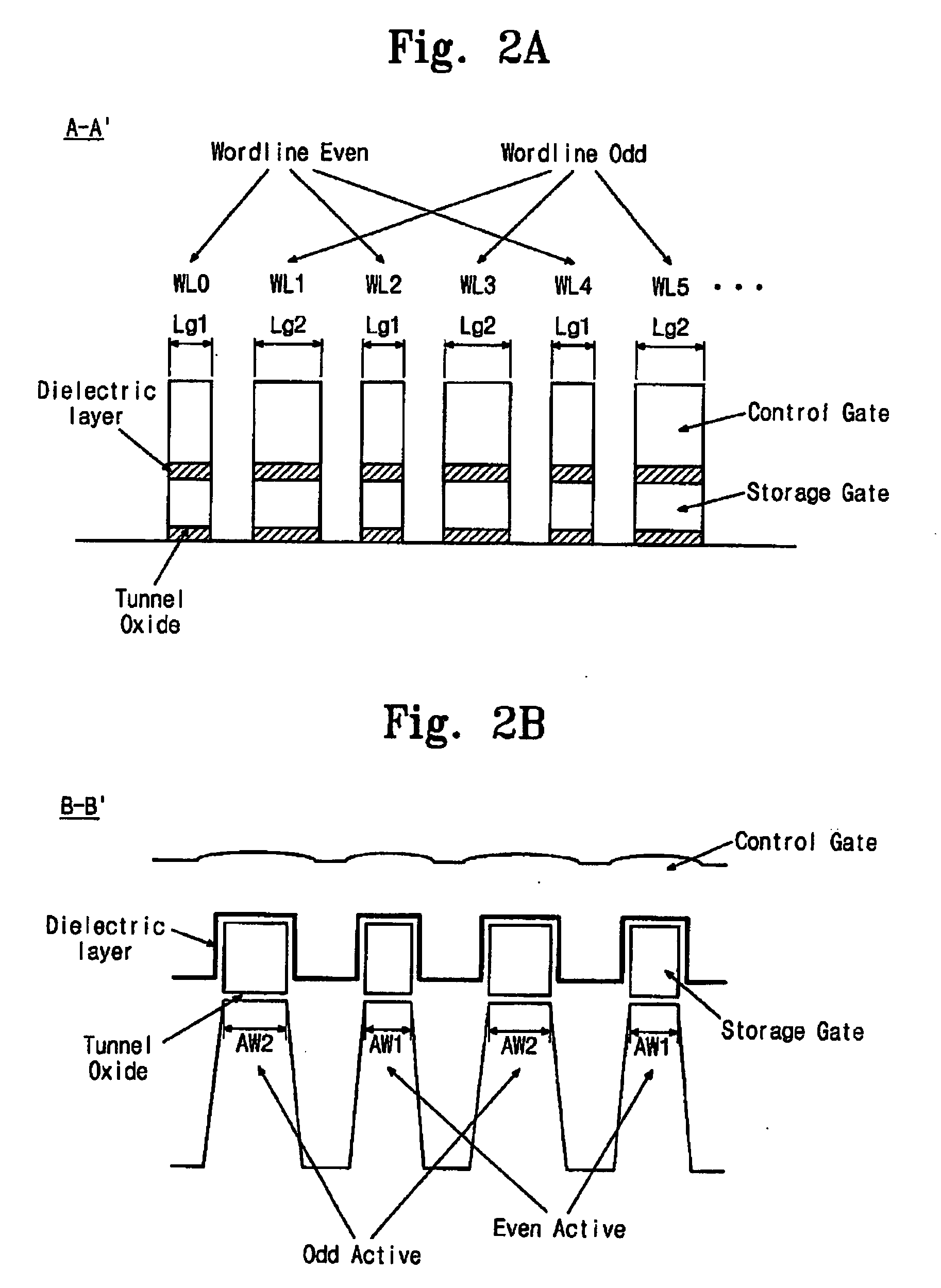
[0038]A nonvolatile memory device may be driven in separate ways suitable for distribution characteristics of memory cells according to whether a memory cell is an even-numbered or odd-numbered cell. Herein, the even number or odd number of the memory cell is determined according to whether a memory cell is connected to an even-numbered or odd-numbered wordline. That is, the memory cell connected to the even-numbered wordline will be referred to as an even-numbered memory cell, and the memory cell connected to the odd-numbered wordline will be referred to as an odd-numbered memory cell, hereinafter.

[0039]FIG. 5 is a functional block diagram of a nonvolatile memory device 100 according to the first embodiment of the present invention. The nonvolatile memory device 100 of FIG. 5 is a NAND flash memory device. However, it is obvious to those skilled in the art that the present invention is also applicable to other memory devices (e.g., mask read only memory (MROM), programmable ROM (P...

second embodiment

[0080]FIG. 12 is a functional block diagram of a nonvolatile memory device 200 according to the present invention. Referring to FIG. 12, the nonvolatile memory device 200 includes a 3-D memory array 210, a decoder 220, a page buffer 230 and control logic 240. The 3-D memory array 210 is as described above with reference to FIG. 11. The nonvolatile memory device 200 includes control logic 240 that is configured to control the memory cells according to whether the memory cell corresponding to an address ADD belongs to the first layer 212 of the memory array 210 or the second layer 214 of the memory array 210. Specifically, the control logic 240 includes a first layer control logic 242 configured to control the memory cells belonging to the first layer 212, and a second layer control logic 244 configured to control the memory cells belonging to the second layer 214.

[0081]FIGS. 13A-13C are graphical illustrations of a programming method of the nonvolatile memory device 200 of FIG. 12. I...


PUM


Abstract

Provided are a nonvolatile memory device and a driving method thereof. In the method of driving a nonvolatile memory device, a structural shape and position of a memory cell to be driven is determined, and then the memory cell is driven with an optimized operating condition according to a distribution of the memory cell using a determination result.

Description

CROSS-REFERENCE TO RELATED APPLICATIONS[0001]This U.S. non-provisional patent application claims priority under 35 U.S.C. §119 of Korean Patent Application Nos. 10-2007-0019772, filed on Feb. 27, 2007, and 10-2007-0090617, filed on Sep. 6, 2007, the entire contents of which are hereby incorporated by reference.BACKGROUND OF THE INVENTION[0002]1. Field of the Invention[0003]The invention disclosed herein relates generally to a nonvolatile memory device, and more particularly, but without limitation, to a method of driving a nonvolatile memory device.[0004]2. Description of the Related Art[0005]Nonvolatile memory devices retain data stored in cells even if power is not supplied. Flash memory devices are one type of nonvolatile memory. Since flash memory devices electrically erase a block of data cells at a time, flash memory devices are being widely used in computers, memory cards, etc.[0006]Such a flash memory device is classified into a NOR flash memory and a NAND flash memory. One ...

Claims


Application Information

Patent Timeline
Patent Type & Authority Applications(United States)
IPC IPC(8): G11C16/06
CPCG11C11/5621G11C16/3454G11C16/30G11C16/10
Inventor PARK, KI-TAEKIM, KI-NAMLEE, YEONG-TAEK
Owner SAMSUNG ELECTRONICS CO LTD
Why Eureka
Try Eureka