Semiconductor device and manufacturing method therefor

a technology of semiconductor devices and manufacturing methods, applied in semiconductor devices, semiconductor/solid-state device details, electrical apparatus, etc., can solve the problems of low polishing rate and high polishing rate generation, insufficient processing shapes, and difficult to maintain the flatness of polished surfaces, so as to reduce the number of manufacturing steps, maintain flatness of polished faces, and process shapes. the effect of sufficien

Inactive Publication Date: 2008-08-28
SHARP KK
View PDF8 Cites 6 Cited by
  • Summary
  • Abstract
  • Description
  • Claims
  • Application Information

AI Technical Summary

Benefits of technology

[0006]An object of the present invention is to provide a manufacturing method for a semiconductor device capable of maintaining flatness of a polished face in the case of embedding interconnections on the surface of an interlayer insulating film and therefore ensuring a sufficiently processed shape of the embedded interconnection structure, and to provide a manufacturing method for a semiconductor device capable of decreasing the number of manufacturing steps for cost reduction.

Problems solved by technology

Consequently, when the second mask thin film is polished in the regions corresponding to both sides of the interconnection groove in this manufacturing method, regions with low polishing rates and high polishing rates are generated inside the surface subject to polishing, and this makes it difficult to maintain the flatness of the polished surface and causes the problem of insufficient processed shapes.
Moreover, a formation process of the second mask thin film made of silicon nitride is necessary, which causes the problem of a large number of steps and high costs.

Method used


Image

  • Semiconductor device and manufacturing method therefor
  • Semiconductor device and manufacturing method therefor
  • Semiconductor device and manufacturing method therefor

Examples


first embodiment

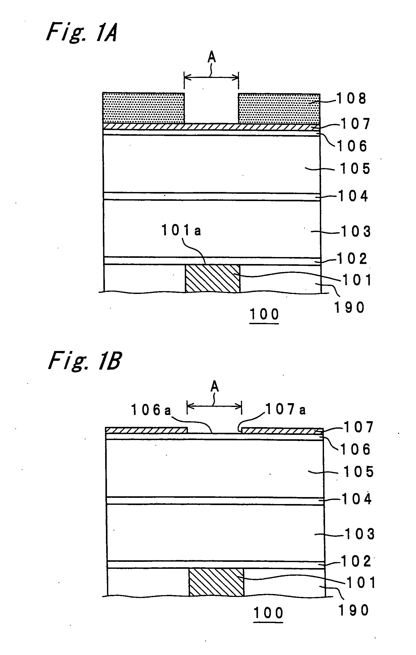
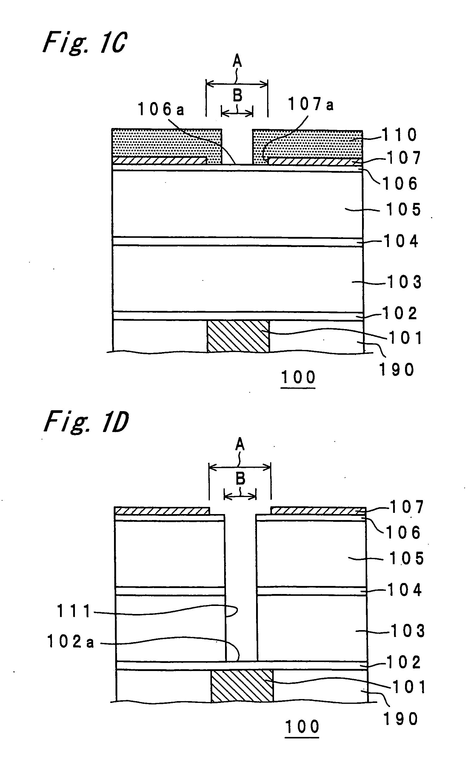
[0070]FIGS. 1A to 1H are cross sectional views showing the steps in a manufacturing method for a semiconductor device in a first embodiment of the present invention.

[0071]As shown in FIG. 1A, an insulating layer 190 is formed in advance on a semiconductor substrate 100, and a lower interconnection 101 is embedded in a portion of the insulating layer 190 corresponding to a specified region A. The width of the lower interconnection 101 is set in the range of 0.05 μm to 200 μm, and an upper face 101a of the lower interconnection 101 and the surface of the insulating layer 190 existing on both sides of the lower interconnection 101 are planar. In the present embodiment, a cap film 102 with a thickness of 10 nm to 50 nm, a first insulating film 103 with a thickness of 100 nm to 500 nm, an etching stopper film 104 with a thickness of 10 nm to 50 nm, and a second insulating film 105 with a thickness of 100 nm to 500 nm are formed in this order on the insulating layer 190 and the lower inte...

second embodiment

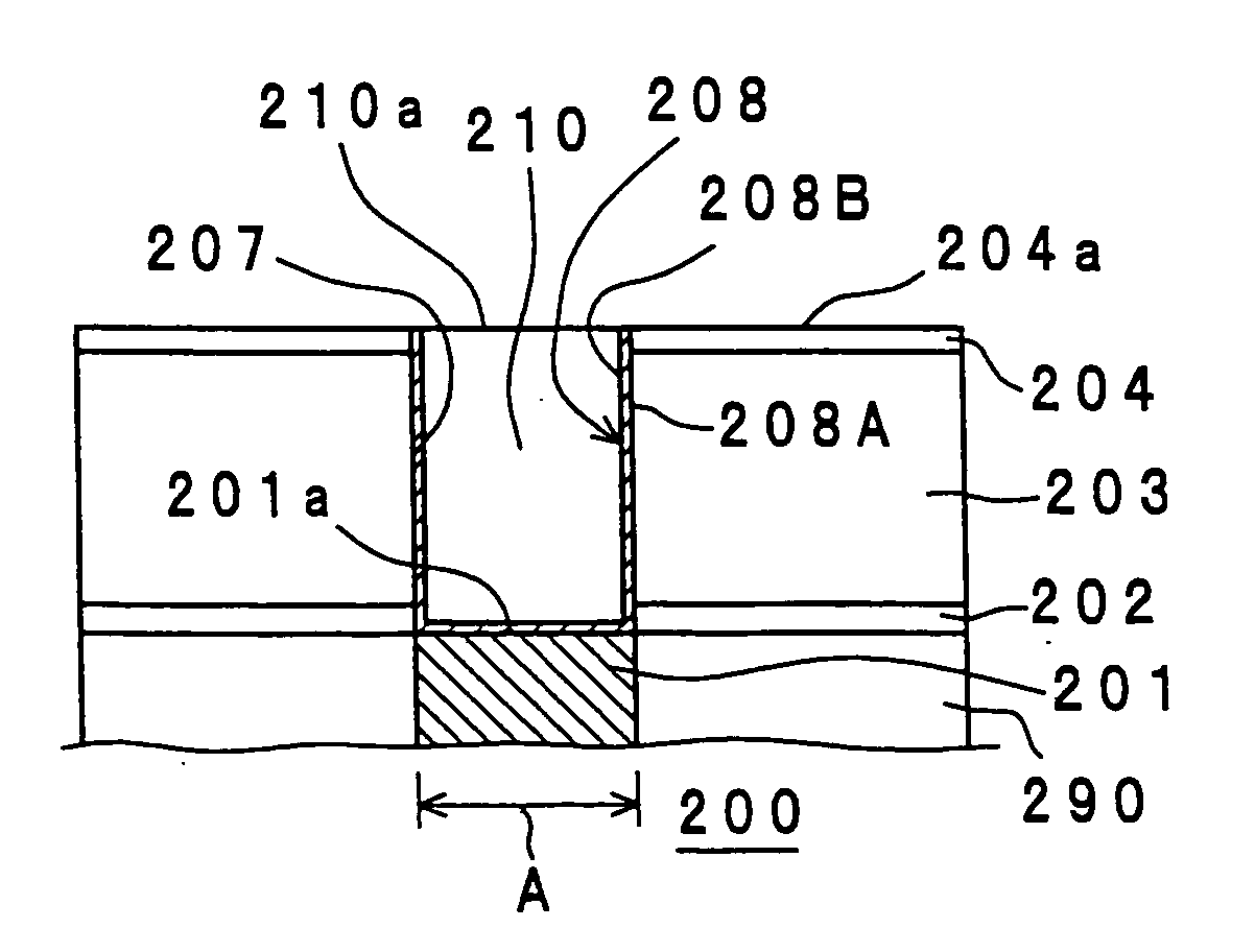
[0089]FIGS. 2A to 2F are cross sectional views showing the steps by a manufacturing method for a semiconductor device in a second embodiment of the present invention.

[0090]As shown in FIG. 2A, an insulating layer 290 is formed in advance on a semiconductor substrate 200, and a lower interconnection 201 is embedded in a portion of the insulating layer 290 corresponding to a specified region A. The width of the lower interconnection 201 is set in the range of 0.05 μm to 20.0 μm, and an upper face 201a of the lower interconnection 201 and the surface of the insulating layer 290 existing on both sides of the lower interconnection 201 are planar. In the present embodiment, a cap film 202 with a thickness of 10 nm to 50 nm and a first insulating film 203 with a thickness of 100 nm to 500 nm are formed in this order on the lower interconnection 201 and the insulating layer 290. Further, on top of these films, a first hard mask 204 with a thickness of 10 nm to 100 nm and a second hard mask ...


PUM


Abstract

In a manufacturing method for a semiconductor storage device, an interlayer insulating film, a first hard mask made of an insulative material for coating the interlayer insulating film and a second hard mask are formed on a substrate. The second hard mask is opened, and with use of the second hard mask as a mask, a recess groove, where an embedded interconnection is to be embedded, is formed in the interlayer insulating film. A diffusion preventing film is formed for preventing an embedded interconnection material from diffusing into the interlayer insulating film. The second hard mask and the diffusion preventing film are made of an identical material, which is a conductive material containing a metallic element in its composition. A conductive metal to be a material of the embedded interconnection is deposited. The surface side of the conductive metal is polished to the level that the first hard mask is exposed therefrom.

Description

CROSS-REFERENCE TO RELATED APPLICATIONS[0001]This Nonprovisional application claims priority under 35 U.S.C. §119(a) on Patent Application No. 2005-165525 filed in Japan on Jun. 6, 2005, the entire contents of which are hereby incorporated by reference.BACKGROUND OF THE INVENTION[0002]The present invention relates to a semiconductor device and a manufacturing method therefor. More specifically, the present invention relates to a manufacturing method for a semiconductor device having an interlayer insulating film with an embedded interconnection structure (damascene structure). The present invention also relates to a semiconductor device manufactured by such a manufacturing method.[0003]Known as a manufacturing method for this kind of semiconductor device is a dual damascene technology involving the processes of forming an interlayer insulating film on a lower interconnection, forming an interconnection groove in which an upper interconnection is to be embedded and a via hole for con...

Claims


Application Information

Patent Timeline
Patent Type & Authority Applications(United States)
IPC IPC(8): H01L21/4763
CPCH01L21/76802H01L23/53238H01L21/7684H01L21/76811H01L2924/0002H01L2924/00H01L21/28H01L21/768H01L21/3205
Inventor TAMURA, KOJI
Owner SHARP KK
Why Eureka
Try Eureka