Check patentability & draft patents in minutes with Patsnap Eureka AI!

Method and apparatus for ultra thin wafer backside processing

a backside processing and ultra-thin technology, applied in the field of wafer processing, can solve the problems of low throughput, risk of wafer breakage, and low throughput during wafer thinning

Active Publication Date: 2008-08-28
ALPHA & OMEGA SEMICON INC
View PDF5 Cites 23 Cited by
  • Summary
  • Abstract
  • Description
  • Claims
  • Application Information

AI Technical Summary

Benefits of technology

[0007]There is therefore a need in the art for a method and apparatus for ultra thin wafer backside processing that overcomes the disadvantages of the prior art. The method and apparatus preferably provide for improved throughput with low risk of wafer breakage. The method and apparatus also preferably provide for wafers of 4 to 2 mils thickness and less at a low cost. The method and apparatus further preferably provide for a high wafer area usage.

Problems solved by technology

However, removal of the carrier usually involves complex operations and thus leads to low throughput as well as the risk of wafer breakage.
However, this approach suffers the disadvantage of having a low throughput during wafer thinning and / or edge ring removal, as well as having a reduced active area (due to the wafer area devoted to the circumference).

Method used


Image

  • Method and apparatus for ultra thin wafer backside processing
  • Method and apparatus for ultra thin wafer backside processing
  • Method and apparatus for ultra thin wafer backside processing

Examples


Embodiment Construction

[0025]The present invention will now be described in detail with reference to the drawings, which are provided as illustrative examples of the invention so as to enable those skilled in the art to practice the invention. Notably, the figures and examples below are not meant to limit the scope of the present invention. Where certain elements of the present invention can be partially or fully implemented using known components, only those portions of such known components that are necessary for an understanding of the present invention will be described, and detailed descriptions of other portions of such known components will be omitted so as not to obscure the invention. Further, the present invention encompasses present and future known equivalents to the components referred to herein by way of illustration.

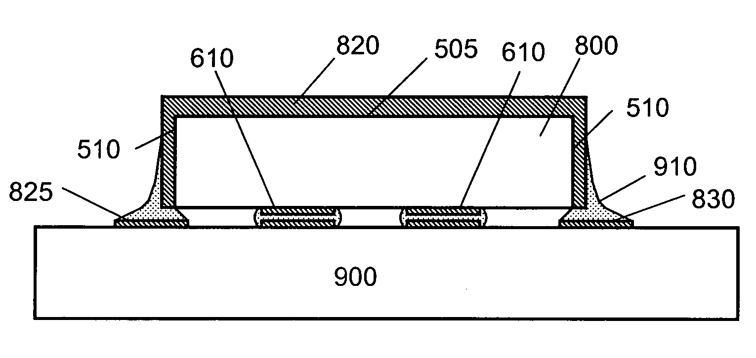
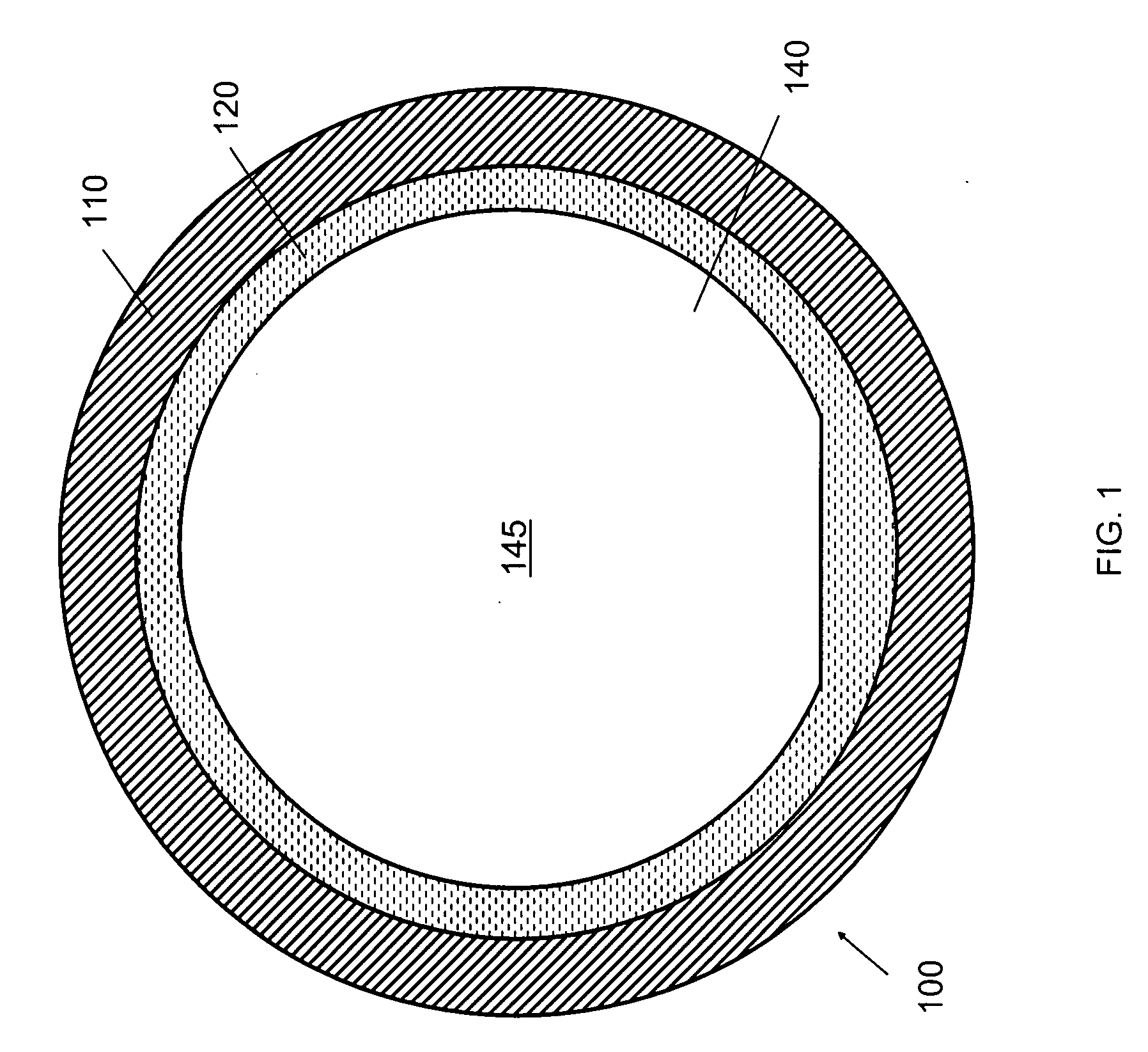
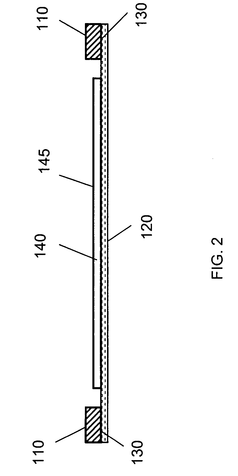
[0026]An apparatus for ultra thin wafer backside processing generally designated 100 is shown in FIG. 1 and FIG. 2. The apparatus 100 comprises an outer ring 110 of generally to...


PUM

PropertyMeasurementUnit
thicknessaaaaaaaaaa
outer diameteraaaaaaaaaa
thicknessaaaaaaaaaa

Abstract

A method and apparatus for ultra thin wafer backside processing are disclosed. The apparatus includes an outer ring holding a high temperature grinding and / or dicing tape to form a support structure. An ultra thin wafer or diced wafer is adhered to the tape within the ring for wafer backside processing. The wafer backside processing includes ion implantation, annealing, etching, sputtering and evaporation while the wafer is in the support structure. Alternative uses of the support structure are also disclosed including the fabrication of dies having metalized side walls.

Description

BACKGROUND OF THE INVENTION[0001]1. Field of the Invention[0002]The present invention relates to wafer processing and more particularly to a method and apparatus for ultra thin wafer backside processing.[0003]2. Description of Related Art[0004]Several factors are driving the trend toward thinner chips having dimensions of less than 4 mils. Such ultra thin chips generally result in lower substrate resistance, allow for the stacking of chips to meet package thickness requirements, and avoid costly thick epitaxial layers in high voltage applications.[0005]Conventionally, a temporary support substrate or carrier can be adhered, usually through an adhesive layer, to the front side of a device wafer to facilitate wafer back grinding and a subsequent thin wafer handling and back side processing. The carrier can be dummy silicon wafer, glass wafer, polymer or polymer based composite substrate, or thick tape. A rigid carrier helps to reduce wafer warping and prevents wafer breakage during ha...

Claims


Application Information

Patent Timeline
Patent Type & Authority Applications(United States)
IPC IPC(8): B24B1/00B05D1/00B24B41/06
CPCB24B7/228B24B41/06H01L2224/16225B28D5/0052H01L24/73B28D5/0011H01L24/05H01L24/06H01L2224/0401H01L2224/0554H01L2224/05568H01L2224/05573H01L2224/06181H01L2224/94H01L2924/00014H01L2224/05599H01L2224/03H01L2224/0555H01L2224/0556
Inventor FENG, TAOSUN, MING
Owner ALPHA & OMEGA SEMICON INC
Features
  • R&D
  • Intellectual Property
  • Life Sciences
  • Materials
  • Tech Scout
  • Unparalleled Data Quality
  • Higher Quality Content
  • 60% Fewer Hallucinations
Learn More