Method for manufacturing circuit modules and circuit module
a manufacturing method and circuit technology, applied in the field of circuit modules, can solve the problems of difficult to provide cutting grooves having a very large depth, inconsistent quality, and reduced productivity, and achieve the effect of excellent shielding properties and easy manufacturing
- Summary
- Abstract
- Description
- Claims
- Application Information
AI Technical Summary
Benefits of technology
Problems solved by technology
Method used
Image
Examples
first preferred embodiment
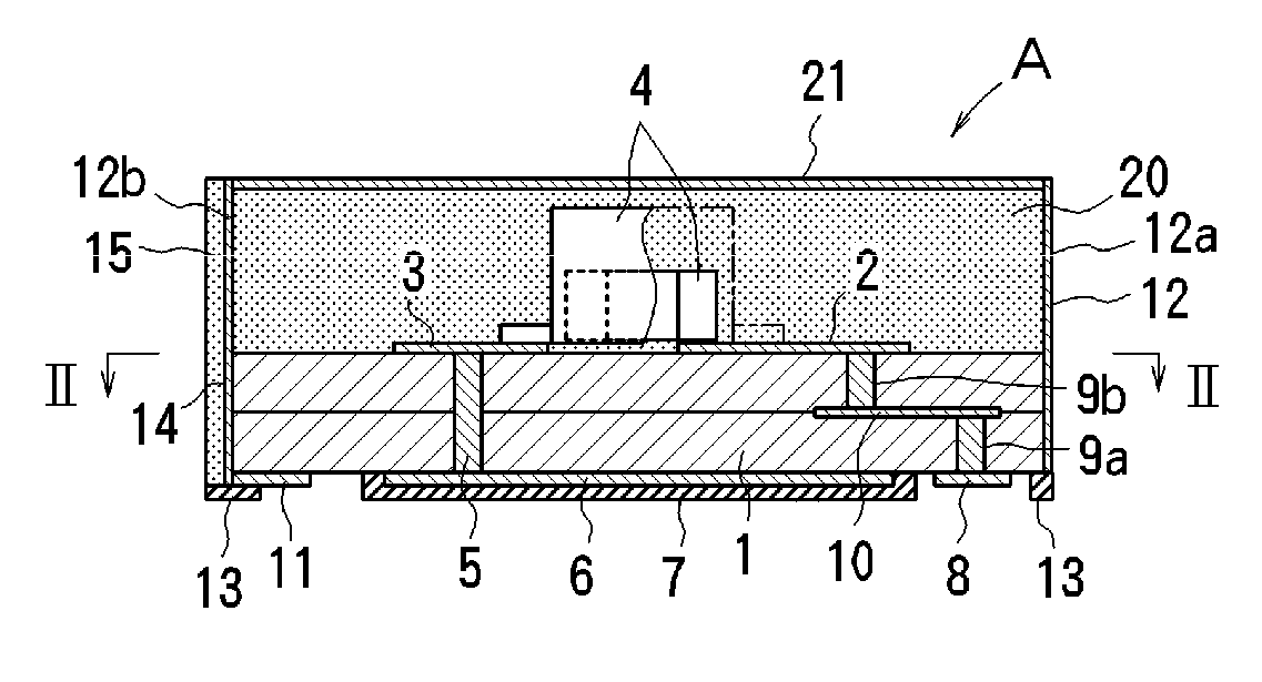
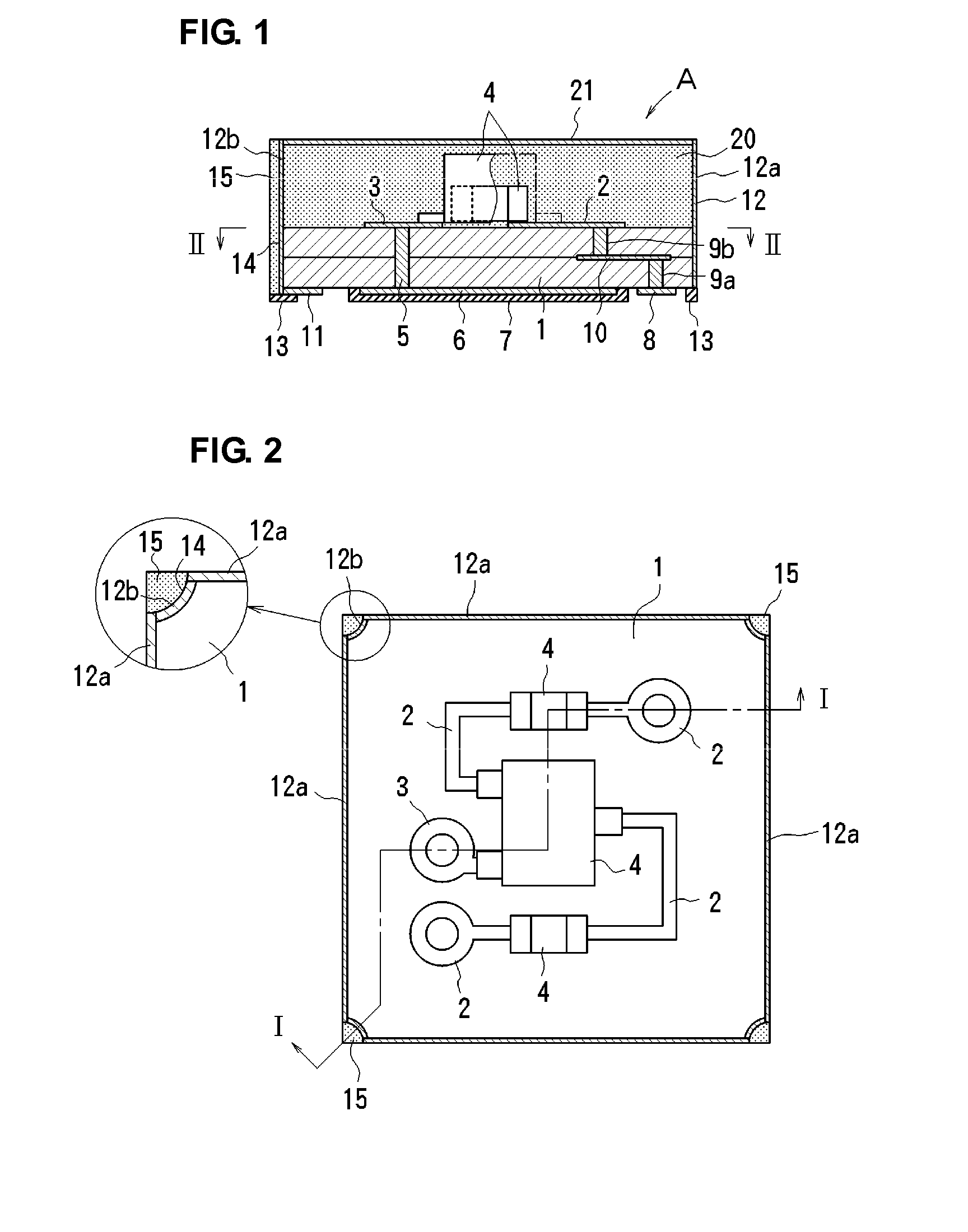
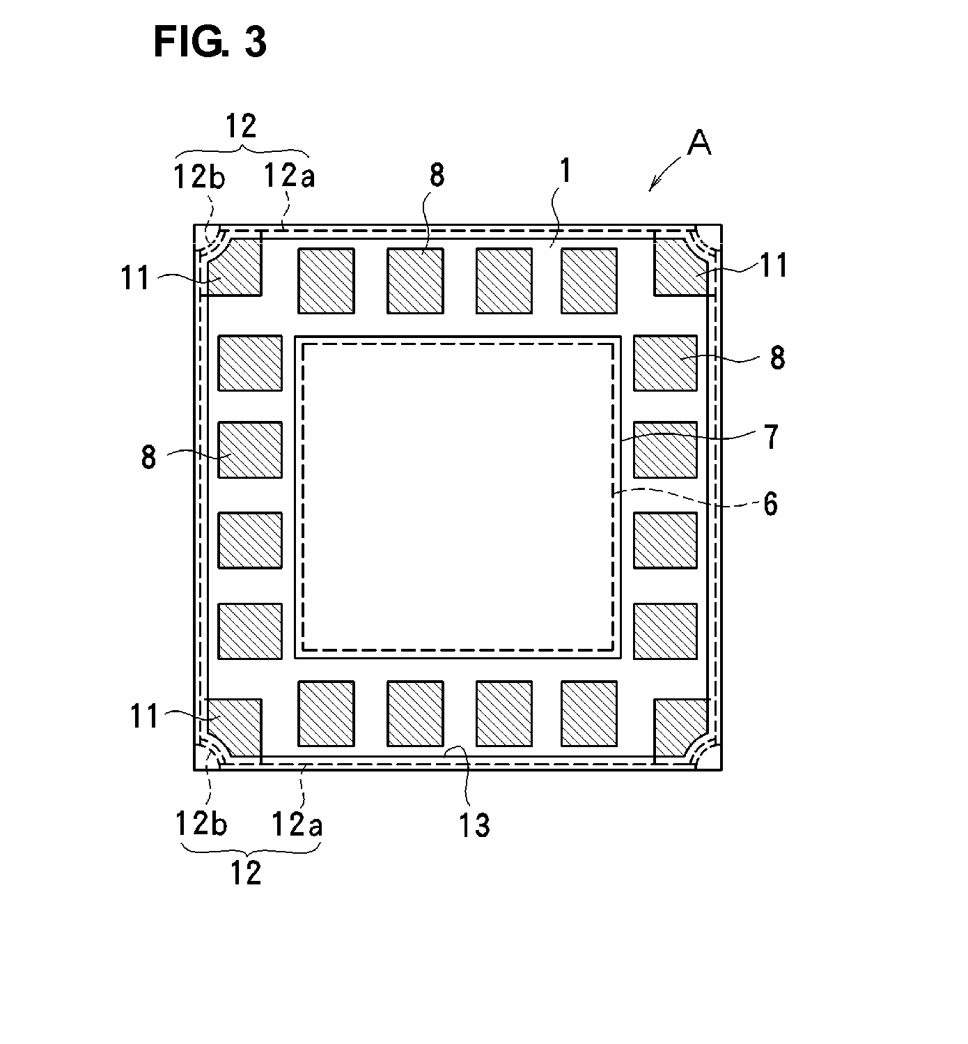
[0044]In FIGS. 1 to 3, a circuit module according to a first preferred embodiment of the present invention is shown. FIG. 1 is a sectional view taken along the step-formed cutting-plane line (the line I-I) of FIG. 2. FIG. 2 is a sectional view taken along the line II-II of FIG. 1. FIG. 3 is a bottom view.
[0045]A circuit module A includes a module substrate 1 that is a substrate having an insulating property, such as a multi-layered resin substrate, and that has a square or substantially square shape, for example. On the top surface of the module substrate 1, wiring electrodes 2, for example, used for inputs and outputs, and a ground electrode 3 are provided. To the electrodes 2 and 3, circuit components 4 including active components, such as transistors used for power amplifiers, and passive components, such as capacitors, are connected. The specific patterns of the wiring electrodes 2 and the ground electrode 3 shown in FIG. 2 are provided only as examples. Additionally, the circui...
second preferred embodiment
[0060]In FIGS. 6 to 8, a circuit module according to a second preferred embodiment is shown. The same elements as those according to the first preferred embodiment and elements corresponding to those according to the first preferred embodiment are denoted by the same reference numerals, and a description thereof is omitted. FIG. 6 is a sectional view taken along the step-formed cutting-plane line (the line VI-VI) of FIG. 7. FIG. 7 is a sectional view taken along the line VII-VII of FIG. 6. FIG. 8 is a bottom view.
[0061]In a circuit module B, electrode films 12c are formed along two opposed sides, and electrode films 12d are formed along the other two sides. The circuit module B is different from the circuit module A in that the side-surface-shielding layers 12 are defined by the electrode films 12c and 12b. Although the electrode films 12c are exposed to the outside, the electrode films 12d are covered by a filling material 30.
[0062]A method for manufacturing the circuit modules B a...
third preferred embodiment
[0070]In FIG. 10, a circuit module according to a third preferred embodiment is shown. The same elements as those according to the first preferred embodiment and elements corresponding to those according to the first preferred embodiment are denoted by the same reference numerals, and a description thereof is omitted. In the first preferred embodiment, after the electrode films 12b are formed on the inner surfaces of the first through holes 16, the first through holes 16 are filled with the filling material 15. However, in the third preferred embodiment, a filling material 40 composed of a conductive adhesive is used so that the filling material 40 can provide both functions.
[0071]Concave grooves 14 are formed in the corner portions of a circuit module C. The concave grooves 14 are filled with the filling material 40, which is composed of a conductive adhesive. The top and bottom ends of the filling material 40 are connected to the top-surface-shielding layer 21 and the ground termi...
PUM
| Property | Measurement | Unit |
|---|---|---|
| thickness | aaaaa | aaaaa |
| conductive | aaaaa | aaaaa |
| width | aaaaa | aaaaa |
Abstract
Description
Claims
Application Information


