Semiconductor device and power receiving device

Inactive Publication Date: 2008-09-04
SEMICON ENERGY LAB CO LTD
View PDF41 Cites 359 Cited by
  • Summary
  • Abstract
  • Description
  • Claims
  • Application Information

AI Technical Summary

Benefits of technology

[0042]A semiconductor device and a power receiving device of the present invention each include a power storage portion, and thus, shortage of electric power for transmitting and receiving individual information, due to deterioration of a battery with time, can be prevented.
[0043]In addition, a semiconductor device and a power receiving device of the present invention include a plurality of antennas and a plurality of rectifier circuits for wirelessly supplying electric power to a power storage portion. Therefore, the power storage portion for supplying electric power for driving the semiconductor device and the power receiving device can be charged by an external electromagnetic wave, without directly connecting the semiconductor device and the power receiving device to a charger. As a result, unlike a conventional active-type RFID tag or the like, it is not necessary to check remaining capacity of a battery or change batteries, so that the semiconductor device and the power receiving device can be continued to be used for long periods of time and over the long term. I

Problems solved by technology

However, as shown in FIG. 3, there has been a problem in that, in an active-type RFID tag, a battery is exhausted with time according to transmission and reception of individual information or strength setting of a radio wave that is needed for transmission and reception thereof, and eventually, electric power that is needed for transmission and reception of individual information cannot be generated.
Therefore, there has been a problem in that remaining capacity of a battery is needed to be checked or changing of batteries is needed for a semiconductor device such as an active-type RFID tag.
In addition, as shown in FIG. 4, there has been a problem in that, in a passive-type RFID tag, transmission to and reception from a long distance or securing of electric power for transmitting radio waves which is needed for transmission and reception of a signal is difficult and realization of a favorable transmission state and reception state is difficult.
Therefore, there has been a problem in that the use of a semiconductor device such as a passive-type RFID tag is limited to the case where distance from an antenna of a reader/writer that is a power supply voltage supply means is close so that supply of electric power can be sufficiently secured by rad

Method used


Image

  • Semiconductor device and power receiving device
  • Semiconductor device and power receiving device
  • Semiconductor device and power receiving device

Examples


embodiment modes

[0084]Embodiment modes of the present invention will be hereinafter explained with reference to the accompanying drawings. However, the present invention can be carried out in many different modes, and it is easily understood by those skilled in the art that modes and details of the present invention can be modified in various ways without departing from the purpose and the scope of the present invention. Therefore, the present invention should not be interpreted as being limited to the description of Embodiment Modes. It is to be noted that, in structures of the present invention hereinafter described, the same portions or portions having similar functions are denoted by the same reference numerals, and repeated explanation thereof will be omitted.

embodiment mode 1

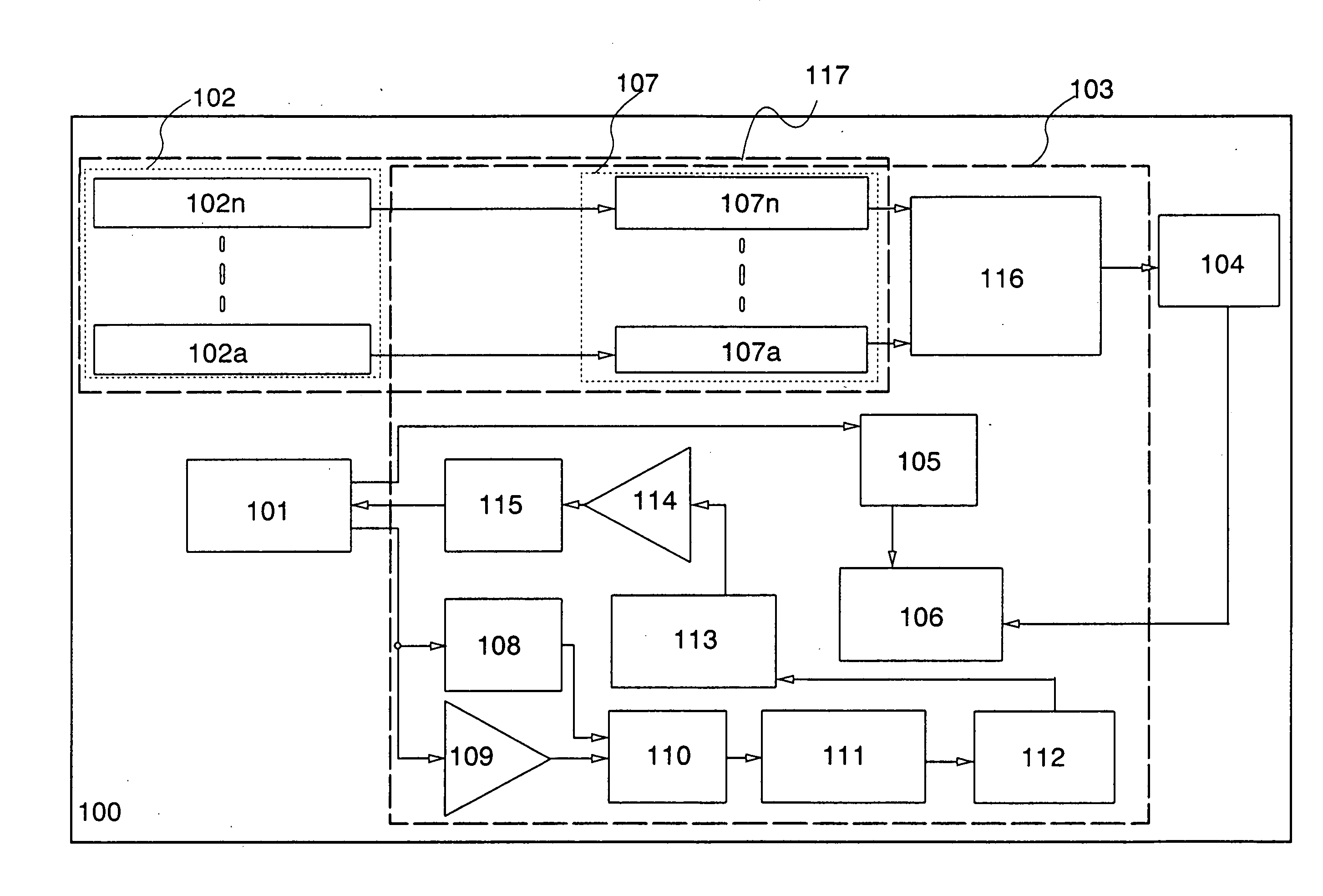
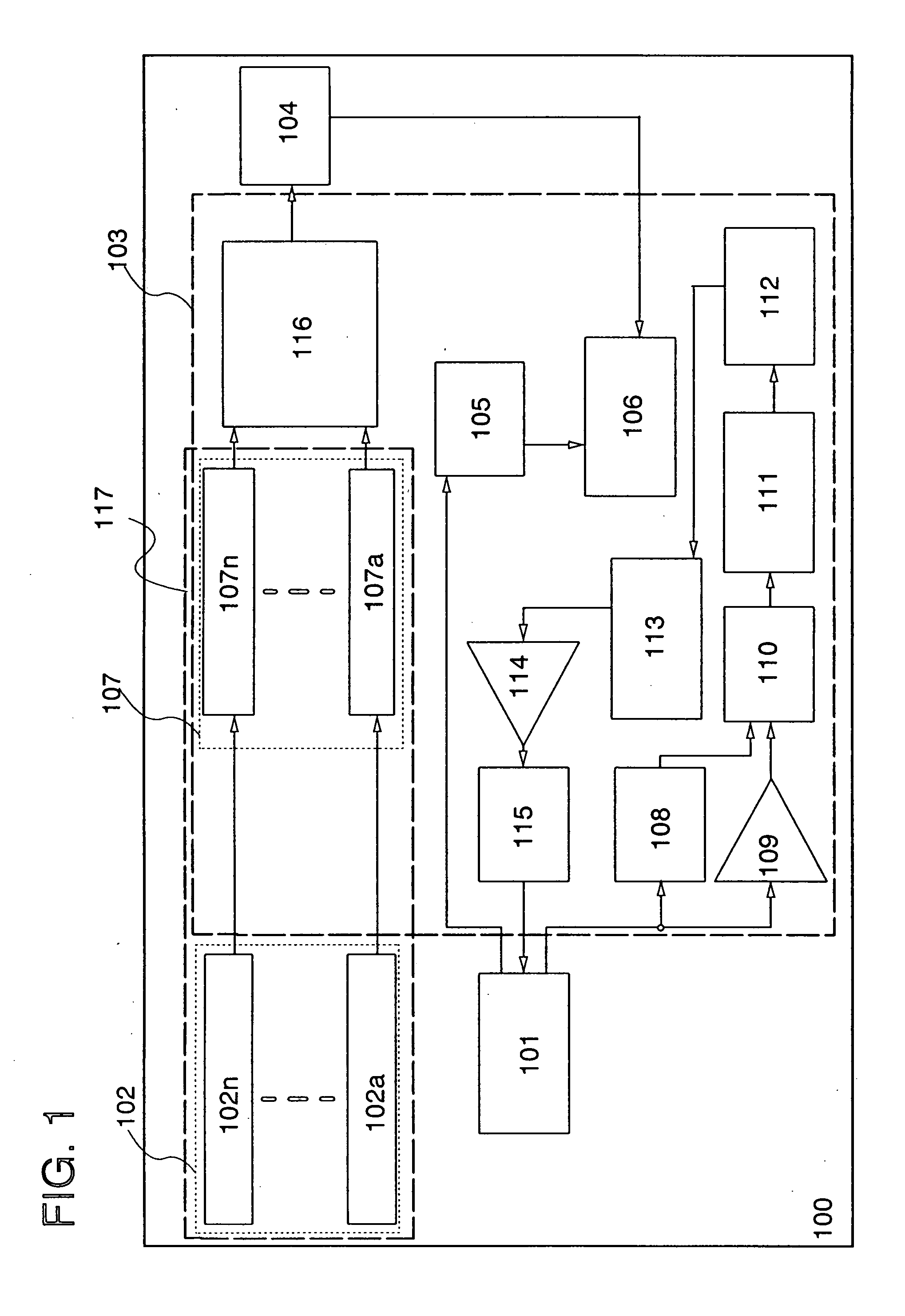
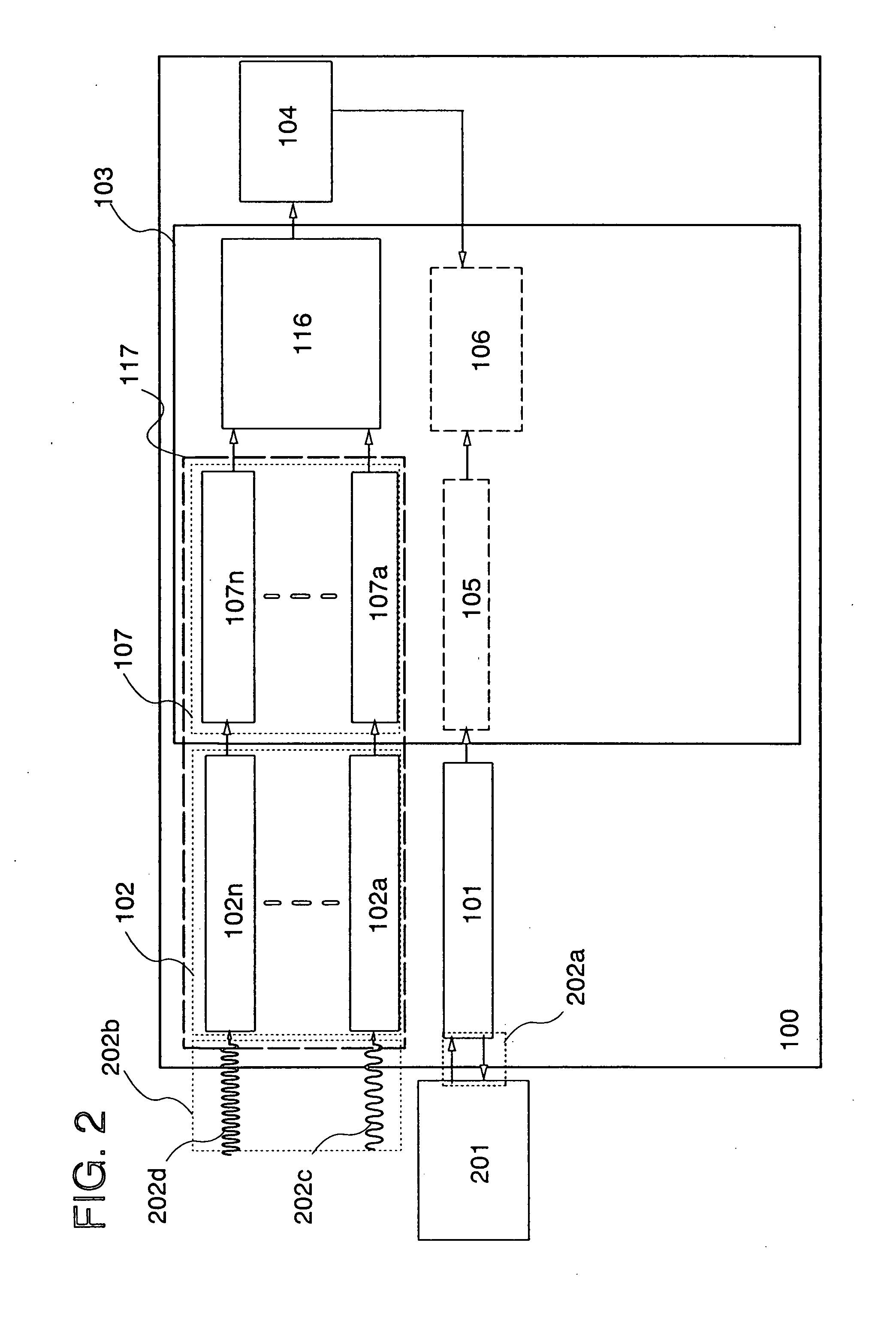
[0085]One structural example of a semiconductor device of the present invention will be explained with reference to block diagrams shown in FIGS. 1 and 2. It is to be noted that, in this embodiment mode, the case of utilizing a semiconductor device as an RFID tag or the like will be explained.

[0086]A semiconductor device 100 shown in FIG. 1 includes a first antenna circuit 101, a signal processing circuit 103, a battery 104, a charging circuit 116, and an antenna-rectifier circuit group 117. The signal processing circuit 103 includes a first rectifier circuit 105, a power supply circuit 106, a demodulation circuit 108, an amplifier 109, a logic circuit 110, a memory control circuit 111, a memory circuit 112, a logic circuit 113, an amplifier 114, and a modulation circuit 115. The antenna-rectifier circuit group 117 includes a pair of N-1 antenna-rectifier circuits including a pair of a second antenna circuit 102a and a second rectifier circuit 107a, or an antenna circuit group 102 a...

embodiment mode 2

[0136]A structure of a movable electronic device having a power receiving device of the present invention will be explained with reference to block diagrams of FIGS. 13 and 14. A power receiving device explained in this embodiment mode is referred to as an RF battery or a wireless battery.

[0137]A movable electronic device 2700 shown in FIG. 13 includes a power receiving portion 2701 and a power supply load portion 2705. The power receiving portion 2701 includes an antenna circuit group 2702 including a plurality of antenna circuits; a signal processing circuit 2703; and a battery 2704. The signal processing circuit 2703 includes a rectifier circuit group 2707 including a plurality of rectifier circuits; a power supply circuit 2708; and a charging circuit 2716. Please note that 2717 denotes an antenna-rectifier circuit group including the rectifier circuit group 2707 and the antenna circuit group 2702.

[0138]It is to be noted that although the power supply circuit 2708 in FIG. 13 supp...


PUM


Abstract

An object is to provide a semiconductor device that is capable of wireless communication, such as an RFID tag, which can transmit and receive individual information without checking remaining capacity of a battery or changing batteries due to deterioration with time in the battery for a drive power supply voltage, and maintain a favorable a transmission/reception state even when electric power of an electromagnetic wave from a reader/writer is not sufficient. The semiconductor device includes a signal processing circuit, a first antenna circuit connected to the signal processing circuit, an antenna circuit group, a rectifier circuit group and a battery connected to the signal processing circuit. The first antenna circuit transmits and receives a signal for transmitting data stored in the signal processing circuit and drives a power supply circuit, and each antenna circuit of the antenna circuit group receives a signal for charging the battery and includes an antenna which has a different corresponding frequency.

Description

BACKGROUND OF THE INVENTION[0001]1. Field of the Invention[0002]The present invention relates to a semiconductor device and a power receiving device. In particular, the present invention relates to a semiconductor device and a power receiving device that transmit and receive data through a radio wave and wirelessly receive electric power.[0003]2. Description of the Related Art[0004]In recent years, an individual identification technology utilizing wireless communication such as radio waves or electromagnetic waves has attracted attention. In particular, as a semiconductor device which transmits and receives data by wireless communication, an individual identification technology utilizing an RFID (Radio Frequency Identification) tag has attracted attention. The RFID tag is also referred to as an IC (Integrated Circuit) tag, an IC chip, an RF (Radio Frequency) tag, a wireless tag, or an electronic tag. The individual identification technology utilizing an RFID tag or the like has star...

Claims


Application Information

Patent Timeline
IPC IPC(8): G06K19/077
CPCG06K19/0701G06K19/0705G06K19/0723G06K19/07783G06K19/07767G06K19/07779G06K19/0724B60L1/00H04B5/0037Y02T90/16G06K19/07773H01L27/1255H01L27/1266H01L2223/6677H02J50/12H02J50/20H02J50/80Y02D30/70
Inventor OSADA, TAKESHITAMURA, HIKARU
Owner SEMICON ENERGY LAB CO LTD
Why Eureka
Try Eureka