Chalcopyrite solar cell and method of manufacturing the same

a solar cell and chalcopyrite technology, applied in the field of chalcopyrite solar cells, can solve the problems of low conversion efficiency, difficult to improve conversion efficiency, and extremely low generation efficiency (conversion efficiency), and achieve the effects of high photoelectric conversion efficiency, reduced dead space, and increased conductive ra

Inactive Publication Date: 2008-09-11
HONDA MOTOR CO LTD
View PDF5 Cites 26 Cited by
  • Summary
  • Abstract
  • Description
  • Claims
  • Application Information

AI Technical Summary

Benefits of technology

[0050]In the invention, a contact electrode in which a light-absorbing layer is reformed so as to increase a conductive rate thereof is formed so that a part of the contact electrode overlaps with an area where a first scribing is performed. A third scribing is performed in a part adjacent to the contact electrode, whereby an upper electrode of one unit cell of the adjacent unit cells is electrically connected to a lower electrode of the other unit cell. Then, a dead space can be reduced while a leak current does not occur. Accordingly, a chalcopyrite solar cell having high photoelectric conversion efficiency can be obtained.
[0051]Further, in the invention, a contact electrode in which the light-absorbing layer is reformed to increase a conductive rate thereof is formed as replaced for a second scribing. A third scribing as an element division scribing is performed so that a part thereof overlaps with the contact electrode portion, whereby a dead space is reduced after securing a connection between a transparent electrode layer and an lower electrode layer. Accordingly, a chalcopyrite solar cell having high photoelectric conversion efficiency can be obtained.

Problems solved by technology

As shown in FIG. 4B, when a part of the second scribing overlaps with the first scribing so as to remove the dead space, cracks occur in the light-absorbing layer and result in leak current.
Since it is difficult to reduce the dead space, it is difficult to improve the conversion efficiency.
Consequently, generation efficiency (conversion efficiency) extremely decreases.
Since it is difficult to reduce the dead space, it is difficult to improve the conversion efficiency.

Method used


Image

  • Chalcopyrite solar cell and method of manufacturing the same
  • Chalcopyrite solar cell and method of manufacturing the same
  • Chalcopyrite solar cell and method of manufacturing the same

Examples


example 1

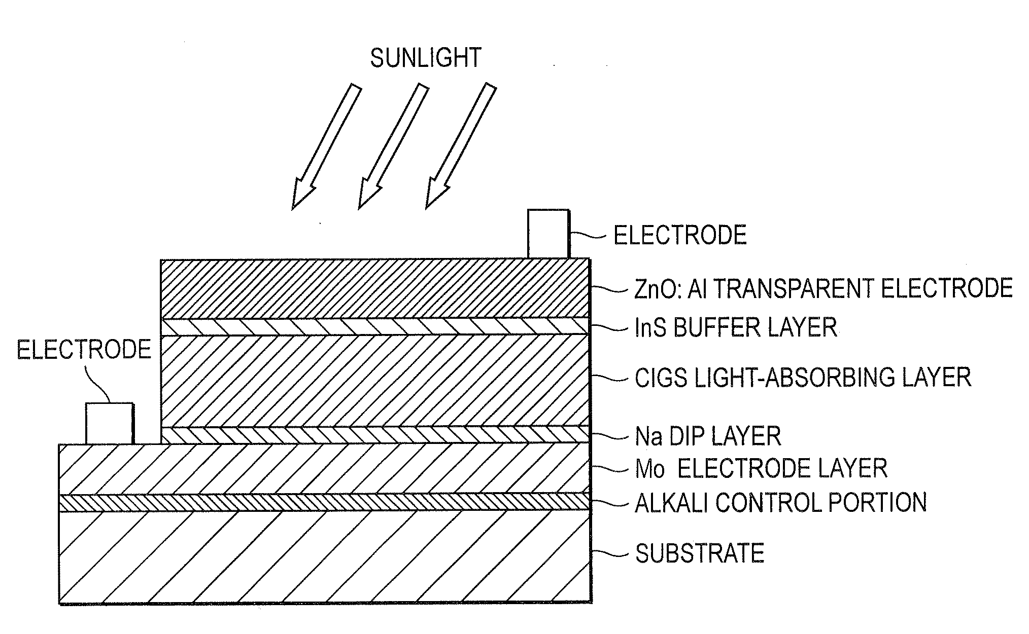
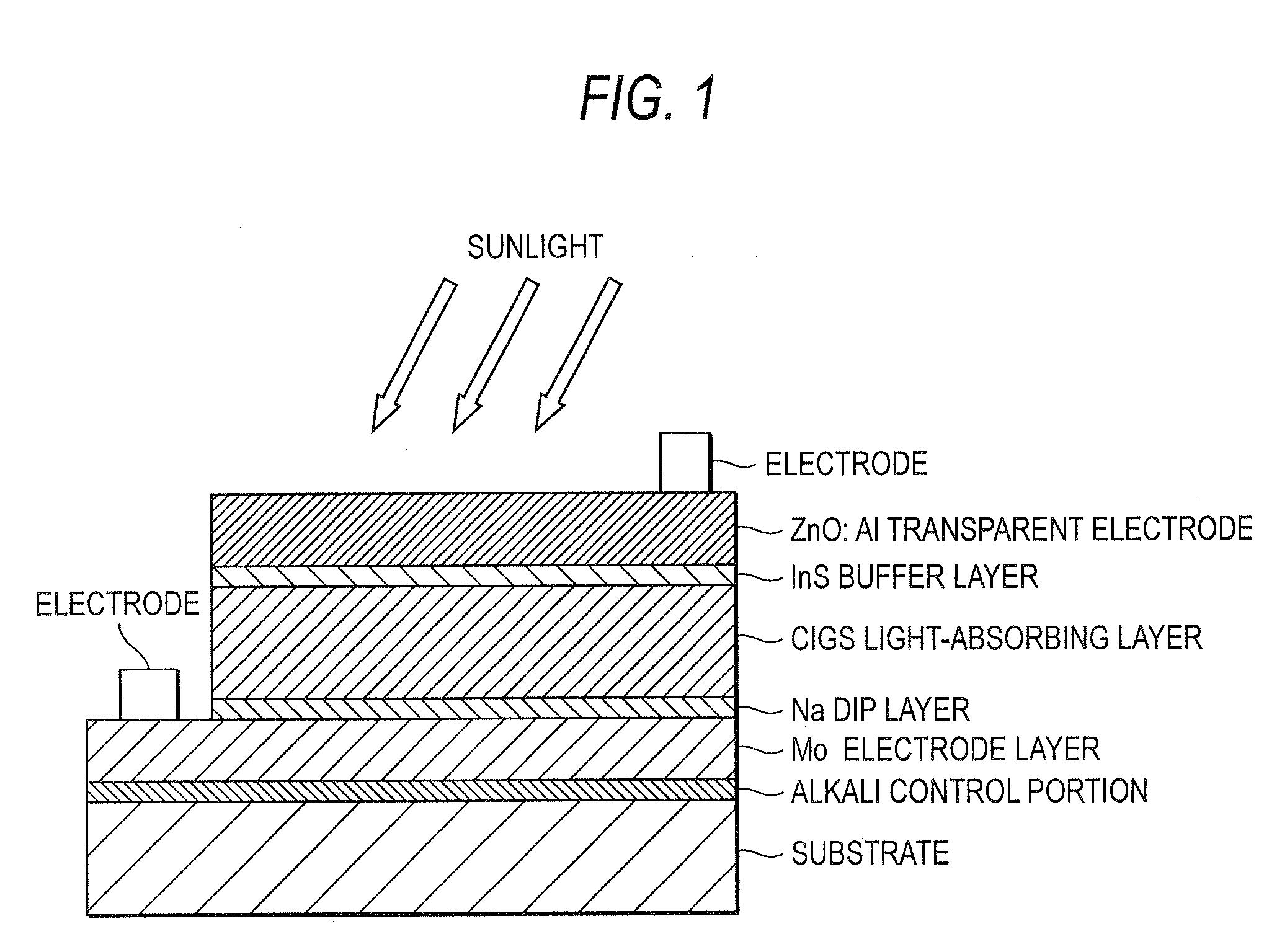
[0069]FIG. 5 is a sectional view illustrating a chalcopyrite solar cell according to the invention. The same reference numerals denote the same parts as the conventional art. In the chalcopyrite solar cell of the invention, a single unit cell (herein, referred to as “a unit cell”) is formed out of a lower electrode layer (Mo electrode layer) 2 formed on a substrate 1, a light-absorbing layer (CIGS light-absorbing layer) 3 including copper, indium, gallium, and selenium, a high-resistance buffer layer thin film 4 formed of InS, ZnS, CdS, and the like on the light-absorbing layer thin film, and an upper electrode thin film (TCO) 5 formed of ZnOAl and the like. In order to connect the unit cell, a part of a contact electrode 6 connecting the upper electrode and the lower electrode is formed to overlap with a dividing line of the lower electrode 2 formed by a first scribing. That is, the contact electrode 6 is formed between the adjacent lower electrodes 2, 2 and on one of the adjacent ...

example 2

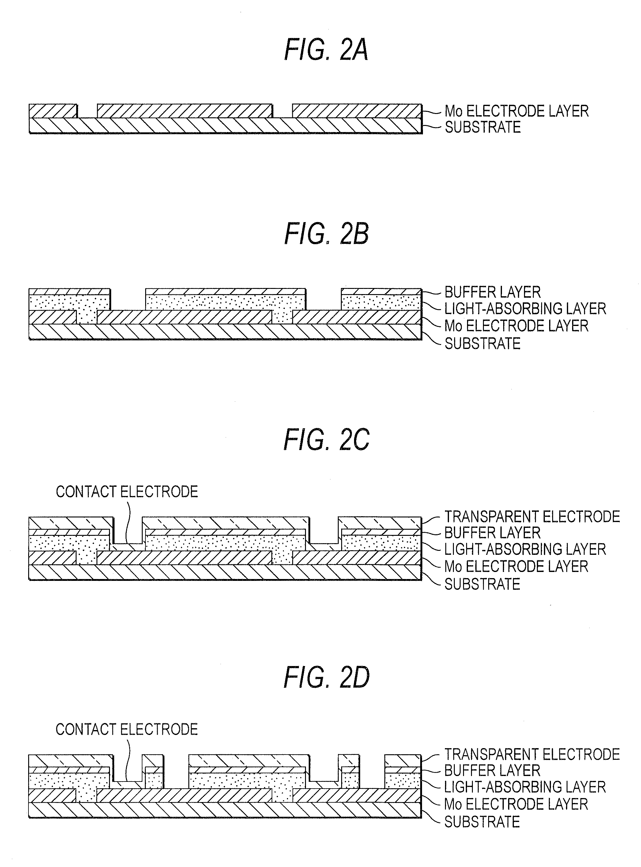
[0096]In the conventional scribing, it is required to perform the second scribing so as to form the dead space at some distance from the scribing line formed by the first scribing and required to perform the third scribing so as to form the dead space at some distance from the second scribing line. However, in the invention, since the contact electrode is formed which the light-absorbing layer is reformed so as to overlap a part thereof to the scribing line formed by the first scribing and the element division scribing (third scribing line) is formed so as to overlap a part thereof to the contact electrode, the monolithic series connection structure can be obtained without forming the dead space. In addition, since the differential level corresponding to the film thickness of the light-absorbing layer does not exist, the transparent electrode is not defeated.

[0097]In the experiment of the inventors, the generation efficiency (conversion efficiency) of the cell improved to about 11.1...

example 3

[0099]FIG. 15 is a sectional view illustrating a chalcopyrite solar cell according to the invention. The same reference numerals denote the same parts as the conventional art. In the chalcopyrite solar cell of the invention, a single unit cell (herein, referred to as “a unit cell”) is formed out of a lower electrode layer (Mo electrode layer) 22 formed on a substrate 21, a light-absorbing layer (CIGS light-absorbing layer) 23 including copper, indium, gallium, and selenium, a high-resistance buffer layer thin film 24 formed of InS, ZnS, CdS, and the like on the light-absorbing layer thin film, and an upper electrode thin film (TCO) 25 formed of ZnOAl and the like. In order to connect the unit cell, a part of a contact electrode connecting the upper electrode and the lower electrode is formed to be adjacent to a dividing line formed by a below-described element division scribing (third scribing). That is, the contact electrode 26 is formed on one lower electrode 22 separated from a s...


PUM


Abstract

A single unit cell (herein, referred to as “a unit cell”) is formed out of a lower electrode layer (Mo electrode layer) 2 formed on a substrate 1, a light-absorbing layer (CIGS LIGHT-ABSORBING LAYER) 3 including copper, indium, gallium, and selenium, a high-resistance buffer layer thin film 4 formed of InS, ZnS, CdS, and the like on the light-absorbing layer thin film, and an upper electrode thin film (TCO) 5 formed of ZnOAl and the like. In order to connect the unit cell, a part of a contact electrode 6 connecting the upper electrode and the lower electrode is formed to overlap with a dividing line of the lower electrode 2 formed by a first scribing.

Description

BACKGROUND OF THE INVENTION[0001]The present invention relates to a chalcopyrite solar cell which is a compound-based solar cell, and more particularly, to a chalcopyrite solar cell and a method of manufacturing the same in which a monolithic series connection structure is formed with a small dead space.[0002]A solar cell which receives light and converts the light into electric energy is classified into a bulk system and a thin film system depending on a thickness of a semiconductor.[0003]The thin film system is a solar cell having a thickness of a semiconductor layer smaller than the range of several 10 μm to several μm, and is classified into an Si thin film system and a compound thin film system. The compound thin film system includes a group II-VI compound group, a chalcopyrite group, and the like. Several kinds of the compound thin film systems are commercialized.[0004]The chalcopyrite solar cell included in the chalcopyrite solar system among them is call as a CIGS (CU(InGa)S...

Claims


Application Information

Patent Timeline
Patent Type & Authority Applications(United States)
IPC IPC(8): H01L31/032H01L31/0264H01L31/18
CPCH01L31/0322H01L31/03923H01L31/0463Y02E10/541Y02P70/50
Inventor AOKI, SATOSHIGOTOU, HIROYUKI
Owner HONDA MOTOR CO LTD
Why Eureka
Try Eureka