Method, apparatus, and system to reduce ground resistance in a pixel array

a technology of ground resistance and array, applied in the field of image sensor devices, can solve the problems of large resistance drop in conventional designs

Active Publication Date: 2008-09-11
APTINA IMAGING CORP
View PDF21 Cites 20 Cited by
  • Summary
  • Abstract
  • Description
  • Claims
  • Application Information

AI Technical Summary

Problems solved by technology

An adverse side effect of utilizing an n-type substrate, or a p−type substrate with an n-epi or n-type implanted layer is that the pixel array lacks a substrate to act as a ground conductor and, therefore, the only ground conductor within the pixel array

Method used


Image

  • Method, apparatus, and system to reduce ground resistance in a pixel array
  • Method, apparatus, and system to reduce ground resistance in a pixel array
  • Method, apparatus, and system to reduce ground resistance in a pixel array

Examples


Embodiment Construction

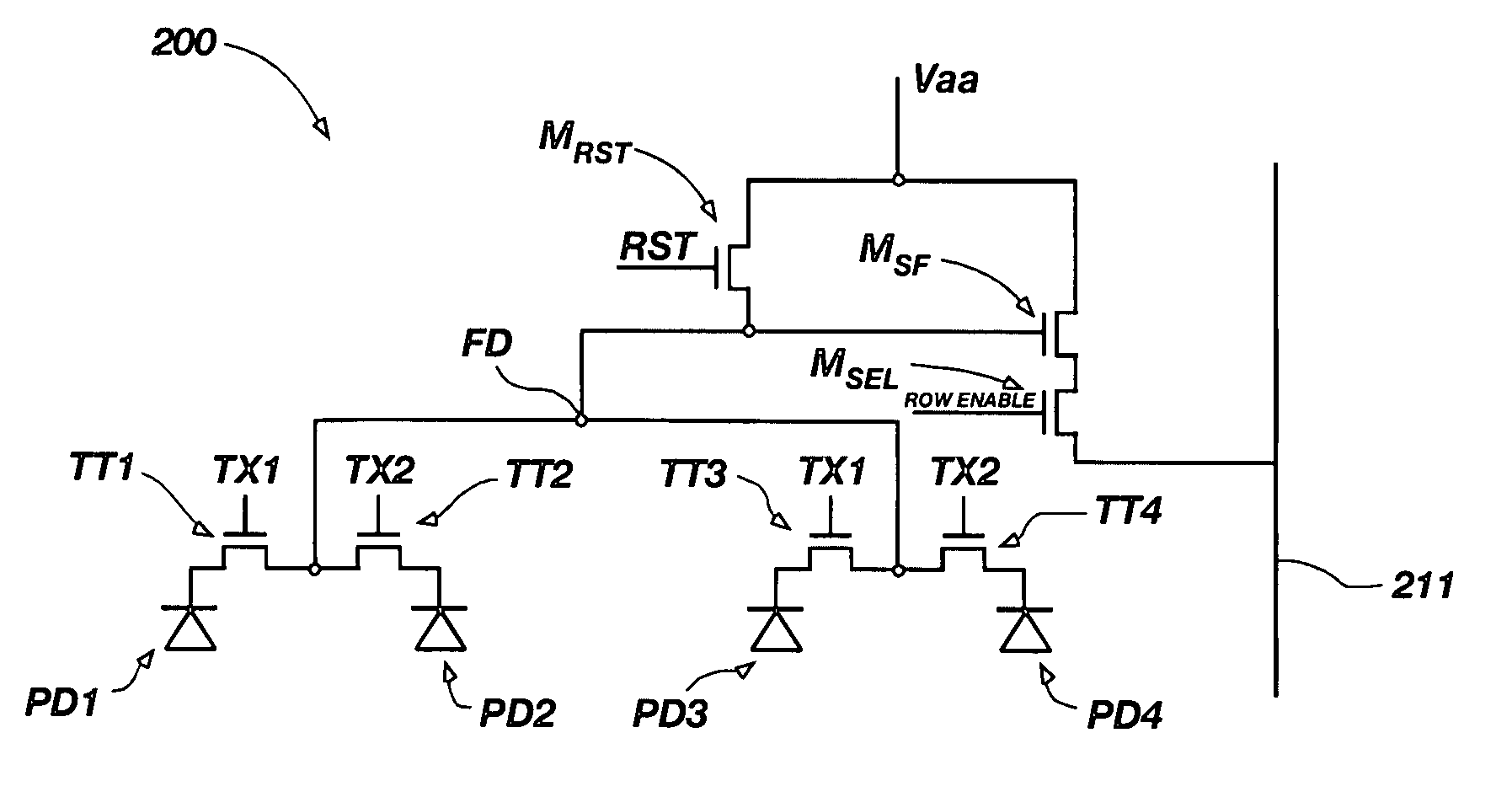
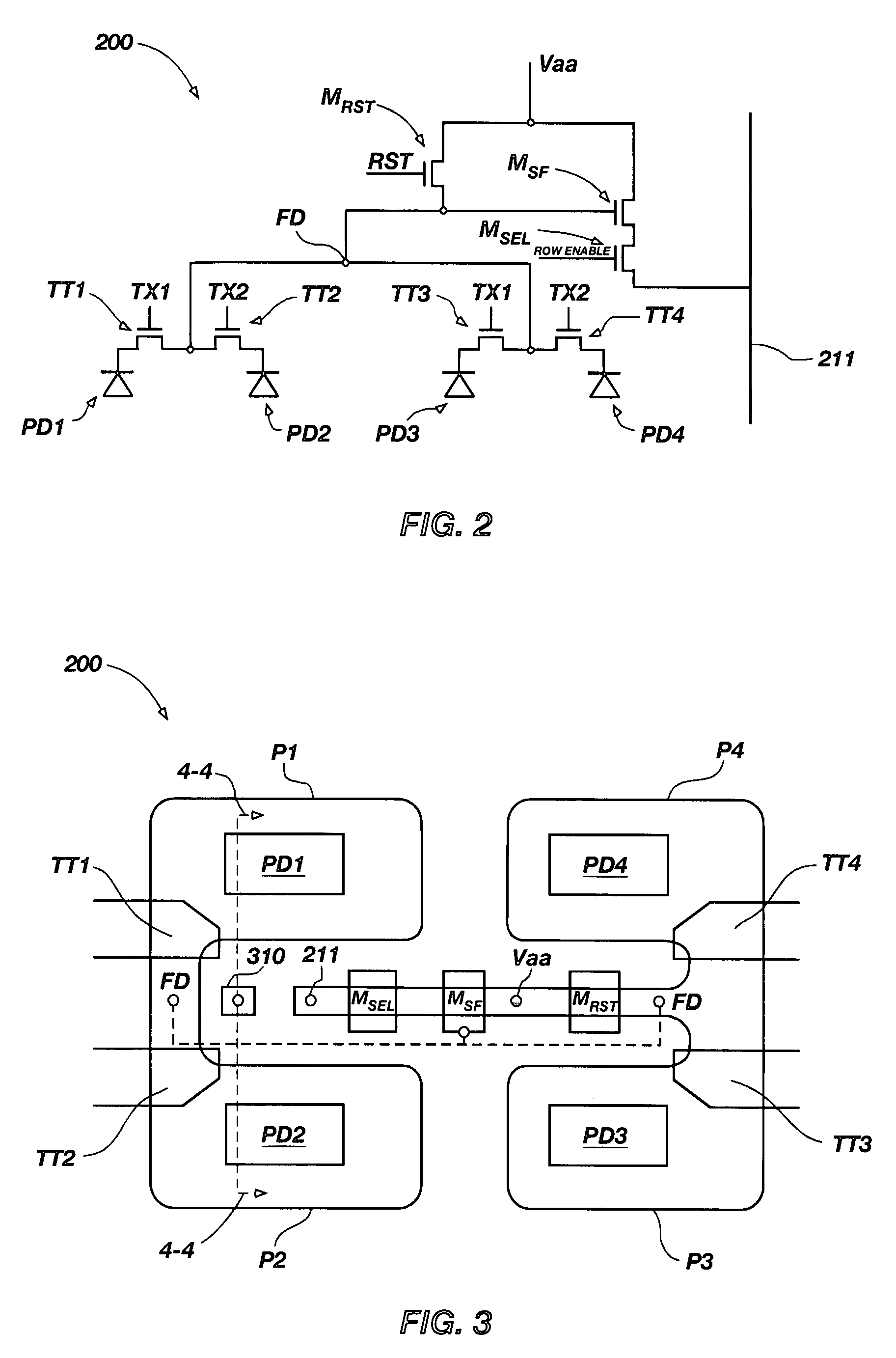
[0017]The present invention, in various embodiments, comprises methods, apparatuses, and systems for an image sensor device including an array of pixels and a ground contact shared by at least two pixels to reduce the ground resistance across a pixel array.

[0018]An embodiment of the invention includes an image sensor device that comprises a substrate and an array of image pixels. Each image pixel of the array is configured for sensing light incident on the image pixel and comprises a photosensitive area within a p−type region for accumulating photo-generated charges within the area. The image sensor device further comprises a plurality of ground contacts operably coupled to the p−type region, at least some ground contacts shared between at least two image pixels of the array. In one embodiment an n-type layer or region may reside between the substrate and the p−type region.

[0019]Another embodiment of the invention includes an electronic system comprising a processor-based device ope...


PUM


Abstract

Methods, devices, and systems for an image sensor device are disclosed. An image sensor device comprises an array of image pixels wherein each pixel is configured for sensing light incident on the pixel. An image sensor device may further comprise a ground contact shared between at least two image pixels of the plurality. The ground contacts may be provided in an even pattern, a random pattern, or a repeating random pattern across the array. The image sensor device may further include an array of shared pixel structures comprising a plurality of pixels, wherein a ground contact may be evenly or randomly placed within each pixel structure across the array of pixel structures.

Description

FIELD OF THE INVENTION[0001]The present invention, in various embodiments, relates generally to an image sensor device and, more specifically, to a pixel array comprising a ground contact operably coupled thereto.BACKGROUND OF THE INVENTION[0002]An image sensor device is a semiconductor device with the capacity to convert an optical image into an electrical signal. Image sensor devices are used in a variety of imaging applications including medical products, navigational equipment, and consumer products such as digital cameras and cellular phones.[0003]Many systems include image sensor devices to sense and capture optical images that can be electronically converted to a digital representation of the image. Image sensor devices include an array of photo-sensitive devices such as photodiodes or photo-transistors fabricated on, for example, a complementary metal oxide semiconductor (CMOS) substrate. Each photo-sensitive device is sensitive to light in such a way that it can create an e...

Claims


Application Information

Patent Timeline
IPC IPC(8): H01L27/148H01L21/77
CPCH01L27/14603H01L27/14683H01L27/1463H01L27/146
Inventor MAURITZSON, RICHARD A.
Owner APTINA IMAGING CORP
Why Eureka
Try Eureka