Current detector circuit and current mode switching regulator

a current mode switching and detector circuit technology, applied in the direction of ac/dc measuring bridges, ignition automatic control, instruments, etc., can solve the problems of complex process and inability to reduce chip sizes, so as to reduce manufacturing costs, simplify the process of current mode switching regulators, and reduce chip sizes

Inactive Publication Date: 2008-09-11
ABLIC INC
View PDF6 Cites 26 Cited by
  • Summary
  • Abstract
  • Description
  • Claims
  • Application Information

AI Technical Summary

Benefits of technology

[0023]By employing the configuration described above, according to the present invention, the second p-channel transistor and the third p-channel transistor are inserted between the first p-channel transistor and the transistor that drives the coil used for voltage conversion, and the terminals of the voltage mirror circuit as detection switches, respectively. As a result, the drain-source voltage of the first p-channel transistor and the transistor that drives the coil can be made to have similar values. Also, because a current corresponding to a transistor ratio flows in the sense resistor, all of the transistors can be constituted by the CMOS structure, instead of forming the transistors as the bipolar transistors or the bi CMOS transistors as in the conventional art. For that reason, the process of the current mode switching regulator semiconductor device is simplified, the chip sizes can be reduced, and the manufacturing costs can be reduced.
[0024]As a result, according to the present invention, the current mode switching regulator can be inexpensively constituted in which the use of the above current sense circuit makes it possible to precisely generate the sense voltage corresponding to the current which flows in the coil, and the output voltage corresponding to the load can be output at a high speed and with a high precision.

Problems solved by technology

However, in the conventional example, because the current detector circuit that detects the current information that is input to the adder 103 generates a very small voltage from a very small current, the current detector circuit is made up of bipolar transistors or bi CMOS transistors (the mixture of bipolar transistors and CMOS transistors), resulting in such drawbacks that the process becomes complicated and the chip sizes cannot be reduced.

Method used


Image

  • Current detector circuit and current mode switching regulator
  • Current detector circuit and current mode switching regulator
  • Current detector circuit and current mode switching regulator

Examples


Embodiment Construction

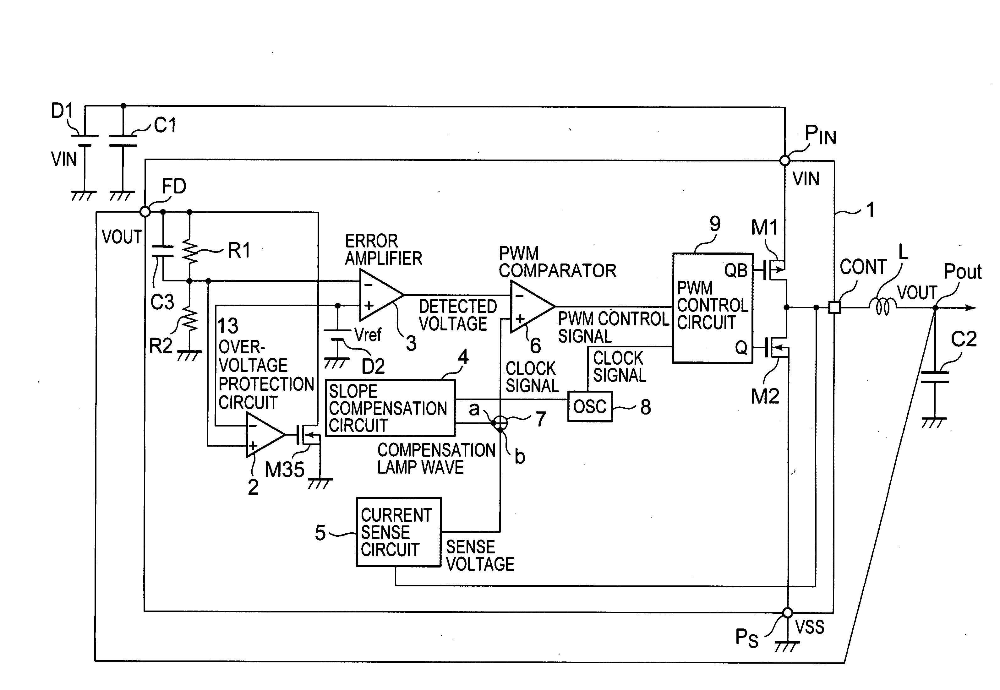
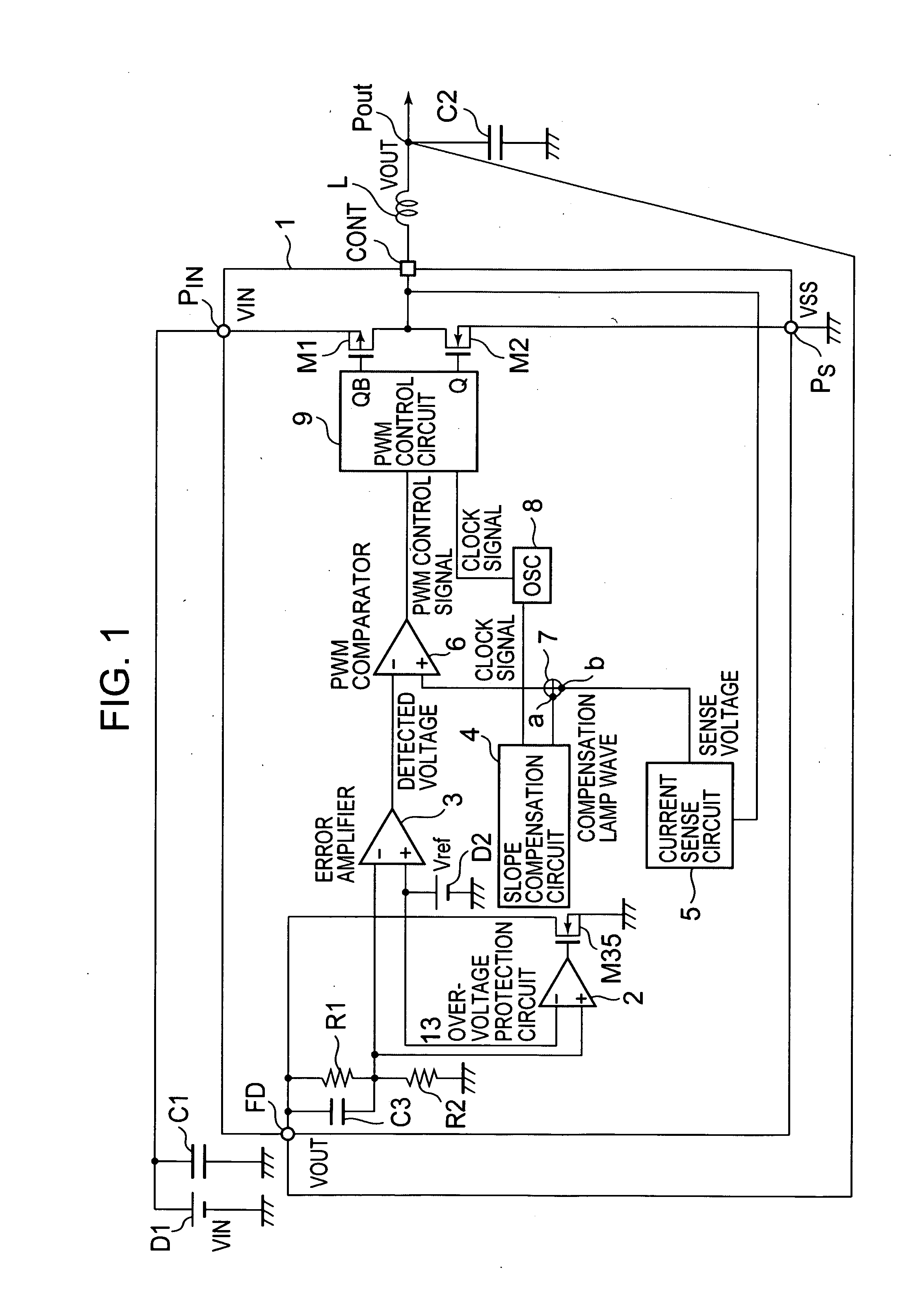
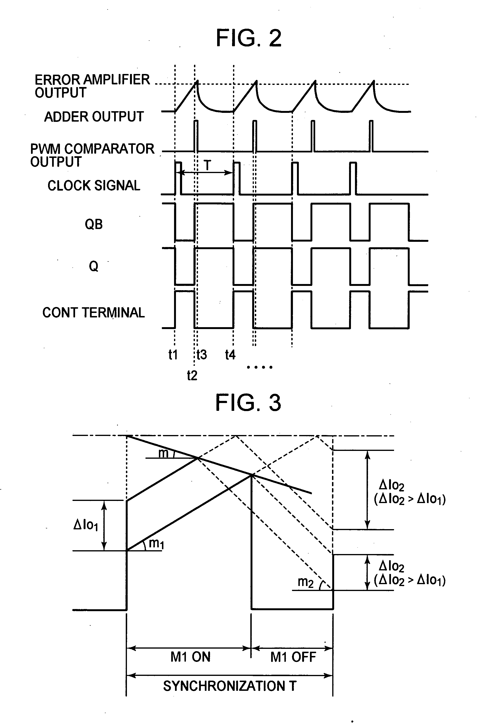
[0031]Hereinafter, a description will be given of a current mode step-down switching regulator semiconductor device 1 using a current sense circuit 5 according to an embodiment of the present invention with reference to the accompanying drawings. FIG. 1 is a block diagram showing a structure example of the current mode step-down switching regulator according to the embodiment of the present invention. The most characteristic structure of the present invention resides in the current detector circuit 5 which is formed of CMOS that measures at a high precision the current flowing in the coil L of the p-channel transistor M1 to be used for controlling the output voltage Vout which is output from the output terminal Pout, and its details will be described.

[0032]In FIG. 1, the current mode step-down switching regulator according to this embodiment is made up of a current mode step-down switching regulator semiconductor device 1, a coil L used for voltage conversion (step-down in this embo...


PUM


Abstract

A current detector circuit is completely formed of CMOS transistors, and is simplified in process, and can be reduced in the chip size. The current detector circuit of the present invention generates a sense voltage that corrects a voltage for slope compensation according to a coil current in a current mode switching regulator. The current detector circuit includes: a first p-channel transistor which allows a current of 1 / N of a current which flows through a transistor that drives a coil to flow therein; a second p-channel transistor having a source connected to a drain of the first p-channel transistor; a third p-channel transistor connected to a drain of a transistor in which the coil current flows; a voltage mirror circuit having one terminal connected to a drain of the second p-channel transistor, and another terminal connected to a drain of the third p-channel transistor, in which voltages at both of the terminals are identical with each other; and a first n-channel transistor having a drain connected to the drain of the first p-channel transistor, and a source grounded through a sense resistor.

Description

BACKGROUND OF THE INVENTION[0001]1. Field of the Invention[0002]The present invention relates to a current mode switching regulator that controls an output voltage on the basis of the detected values of the output voltage and an output current by the aid of a DC input power supply, and a current detector circuit used for the switching regulator.[0003]2. Description of the Related Art[0004]A circuit structured as shown in FIG. 5 is used for a current mode step-down switching regulator (for example, refer to JP 2002-281742 A).[0005]In the circuit, when a switch 107 is turned on, a current flows into a coil 108 from a power supply with the result that an input voltage Vi is accumulated in the coil 108 as an electric energy (that is, electric charges), and also accumulated in an output capacitor 112. Also, when the switch 107 is turned off, the electric energy that has been accumulated in the output capacitor 112 is discharged through a load.[0006]Accordingly, in the current mode step-d...

Claims


Application Information

Patent Timeline
Patent Type & Authority Applications(United States)
IPC IPC(8): G05F1/10G01R19/00
CPCG01R19/0092H02M2001/0025H02M2001/0009H02M3/156H02M1/0009H02M1/0025G05F3/24
Inventor UEHARA, OSAMU
Owner ABLIC INC
Why Eureka
Try Eureka