Thin film transistor and organic light-emitting display device having the thin film transistor

a thin film transistor and display device technology, applied in the direction of semiconductor devices, basic electric elements, electrical appliances, etc., can solve the problems of deteriorating physical properties of the thin film transistor, the difficulty of using the semiconductor layer as a drive circuit of the display panel demanding a high operation speed, and the deterioration of the contact characteristics between the cathode electrode and the light emission layer

Inactive Publication Date: 2008-09-18
SAMSUNG MOBILE DISPLAY CO LTD
View PDF5 Cites 3954 Cited by
  • Summary
  • Abstract
  • Description
  • Claims
  • Application Information

AI Technical Summary

Benefits of technology

[0014]Yet another aspect of the present invention is achieved by providing an organic light-emitting display device including a substrate, a thin film transistor including a semiconductor layer, a gate electrode and a source/drain electrode formed on the substrate, and an organic light emitting diode formed on the thi

Problems solved by technology

However, if a semiconductor layer is formed of the amorphous silicon, it is difficult to use semiconductor layer as a drive circuit of a display panel demanding a high operation speed due to the low mobility.
The poly silicon has a high mobility, but should have a separate compensation circuit due to the non-uniform threshold voltage.
Also, leakage electric current is caused if the thin film transistor using the amorphous or poly silicon as the semiconductor layer is irradiated with the light, resulting in deteriorating physical properties of the thin film transistor.
However, the con

Method used


Image

  • Thin film transistor and organic light-emitting display device having the thin film transistor
  • Thin film transistor and organic light-emitting display device having the thin film transistor
  • Thin film transistor and organic light-emitting display device having the thin film transistor

Examples


first embodiment

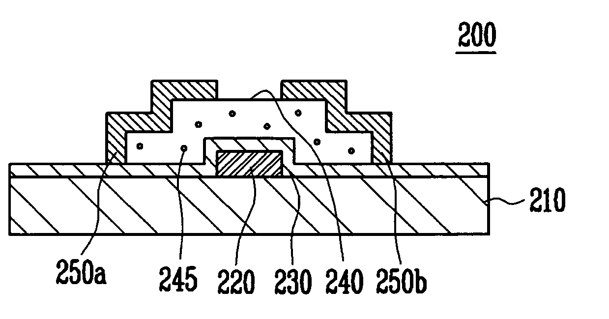
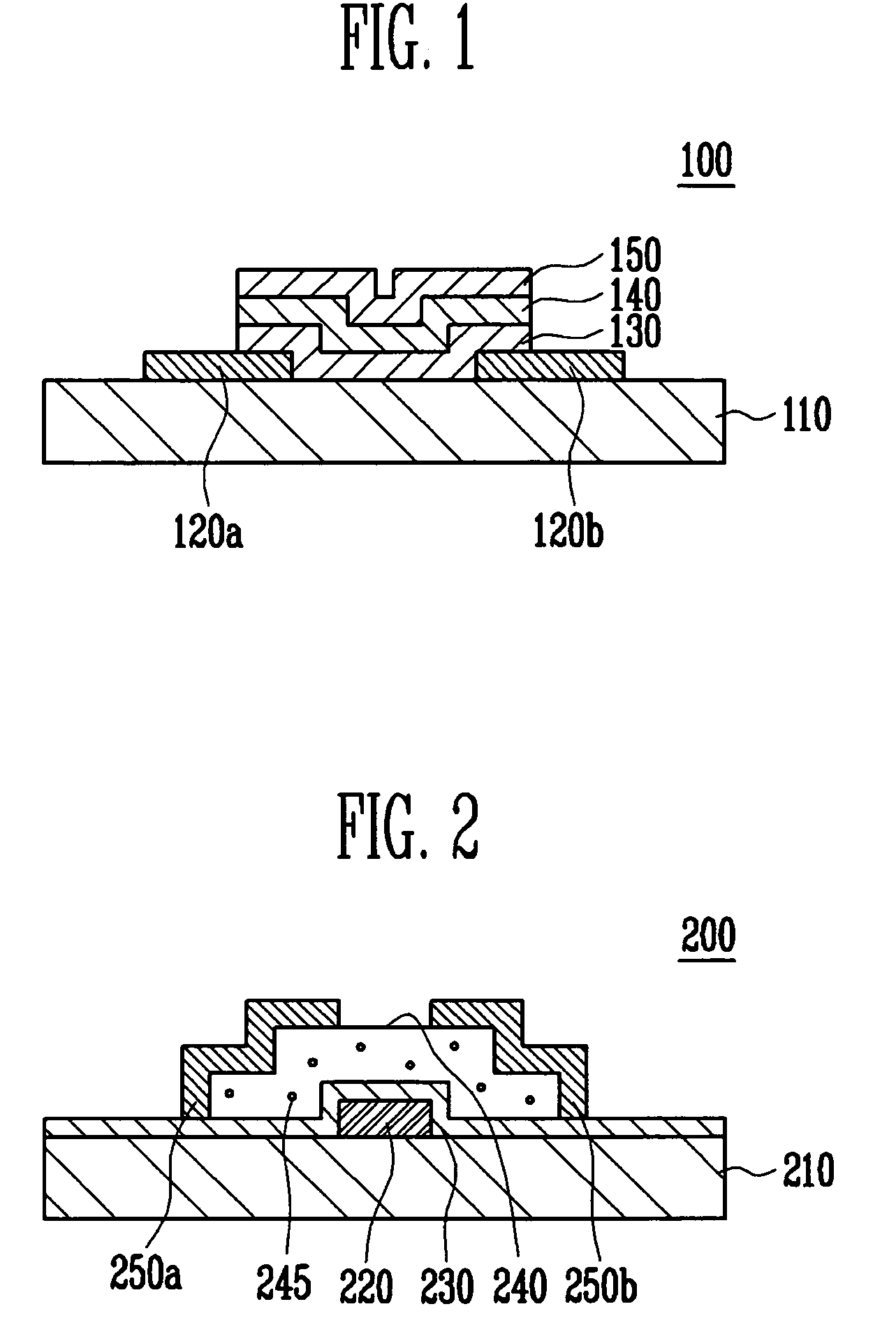
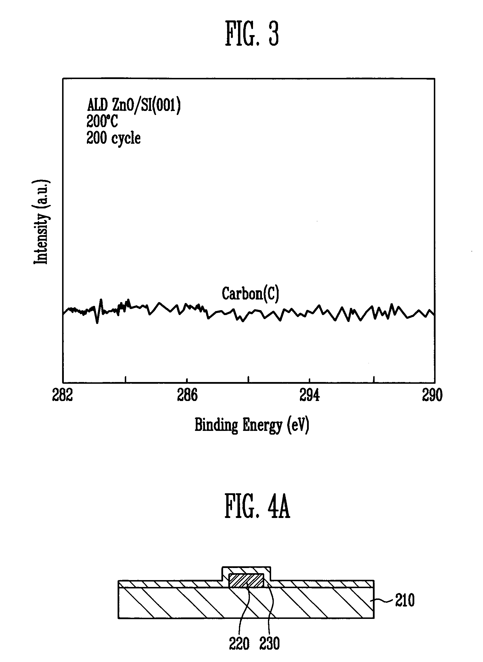
[0026]FIG. 2 is a cross-sectional view showing a thin film transistor constructed as the present invention. Referring to FIG. 2, the thin film transistor 200 of the present invention includes a gate electrode 220 formed on a substrate 210, a gate dielectric layer 230 formed on the substrate 210 covering the gate electrode 220, a semiconductor layer 240 including a channel region, a source region and a drain region and formed on the gate dielectric layer 230, and a source electrode 250a and a drain electrode 250b patterned on the semiconductor layer 240. The source electrode 250a is electrically coupled to the source region of the semiconductor layer 240, and the drain electrode 250b is electrically coupled to the drain region of the semiconductor layer 240. The semiconductor layer 240 is formed of P-type ZnO:N layers through a reaction of a mono-nitrogen gas with a zinc precursor including organic compounds, and the ZnO:N layer includes an impurity element 245 at a content of 3 at %...

second embodiment

[0053]FIG. 6 is a cross-sectional view showing a thin film transistor constructed as the present invention. Referring to FIG. 6, the thin film transistor 400 of to the present invention includes a substrate 410, and a semiconductor layer 420, a gate electrode 440 and source / drain electrodes 470a and 470b formed on the substrate 410. The semiconductor layer 420 is composed of P-type ZnO:N layers 420 through a reaction of a mono-nitrogen gas with a zinc precursor including halide compounds, and the ZnO:N layer 420 includes an halide 425 at a content of 3 at % or less.

[0054]The semiconductor layer 420 is composed of P-type semiconductors. The semiconductor layer 420 is formed of P-type ZnO:N layers by reacting a mono-nitrogen reaction gas with a zinc precursor, namely one organic compound precursor including carbon compounds and selected from the group consisting of DEZ (Diethyl-Zinc), DMZ (Dimethyl-Zinc) and EMZ (Ethyl-Methyl-Zinc), or one inorganic precursor, namely one precursor inc...


PUM


Abstract

Disclosed is a thin film transistor including a P-type semiconductor layer, and an organic light-emitting display device having the thin film transistor. The present invention provides a thin film transistor including a substrate, a semiconductor layer, and a gate electrode and a source/drain electrode formed on the substrate, wherein the semiconductor layer is composed of P-type ZnO:N layers through a reaction of a mono-nitrogen gas with a zinc precursor, and the ZnO:N layer includes an un-reacted impurity element at a content of 3 at % or less.

Description

CLAIM OF PRIORITY[0001]This application makes reference to, incorporates the same herein, and claims all benefits accruing under 35 U.S.C. §119 from an application for THIN FILM TRANSISTOR AND ORGANIC LIGHT-EMITTING DISPLAY DEVICE HAVING THE THIN FILM TRANSISTOR earlier filed in the Korean Intellectual Property Office on the 14th of Mar. 2007 and there duly assigned Serial No. 10-2007-0025062.BACKGROUND OF THE INVENTION[0002]1. Field of the Invention[0003]The present invention relates to a thin film transistor and an organic light-emitting display device having the thin film transistor, and more particularly to a thin film transistor including a P-type semiconductor layer, and an organic light-emitting display device having the thin film transistor.[0004]2. Description of the Related Art[0005]Generally, a semiconductor layer using amorphous silicon or poly silicon has been widely used as the thin film transistor used in an organic light-emitting display device. However, if a semicon...

Claims


Application Information

Patent Timeline
IPC IPC(8): H01L29/22H01L21/34
CPCH01L21/02554H01L21/02579H01L29/7869H01L27/3244H01L21/0262H10K59/12H01L21/02403
Inventor PARK, JIN-SEONGMO, YEON-GONJEONG, JAE-KYEONGJEONG, JONG-HANSHIN, HYUN-SOOLEE, HUN-JUNG
Owner SAMSUNG MOBILE DISPLAY CO LTD
Why Eureka
Try Eureka