Interlaced rtd sensor for zone/average temperature sensing

a technology of zone/average temperature and sensor, applied in the direction of positive temperature coefficient thermistors, heat measurement, instruments, etc., can solve the problems of non-measured temperature, direct affecting process variability and ultimately device performance, and persisting non-uniformity in heat applied to the wafer, so as to improve the wafer processing history and improve reliability. the effect of repeatability and accuracy

Inactive Publication Date: 2008-09-18
SOKUDO CO LTD
View PDF17 Cites 30 Cited by
  • Summary
  • Abstract
  • Description
  • Claims
  • Application Information

AI Technical Summary

Benefits of technology

[0015]Many benefits are achieved by way of the present invention over conventional techniques. For example, embodiments of the present invention provide temperature measurements of semiconductor wafers and bakeplates with improved reliability, repeatability and accuracy. Additionally, embodiments of the present invention provide for improved wafer processi

Problems solved by technology

Lithography type device fabrication processes can be especially sensitive to variations in process recipe variables and the timing between the recipe steps, which directly affects process variability and ultimately device performance.
For example, techniques that measure temperatures only at selected locations near the wafer may not measure temperatures at many locati

Method used


Image

  • Interlaced rtd sensor for zone/average temperature sensing
  • Interlaced rtd sensor for zone/average temperature sensing
  • Interlaced rtd sensor for zone/average temperature sensing

Examples


Embodiment Construction

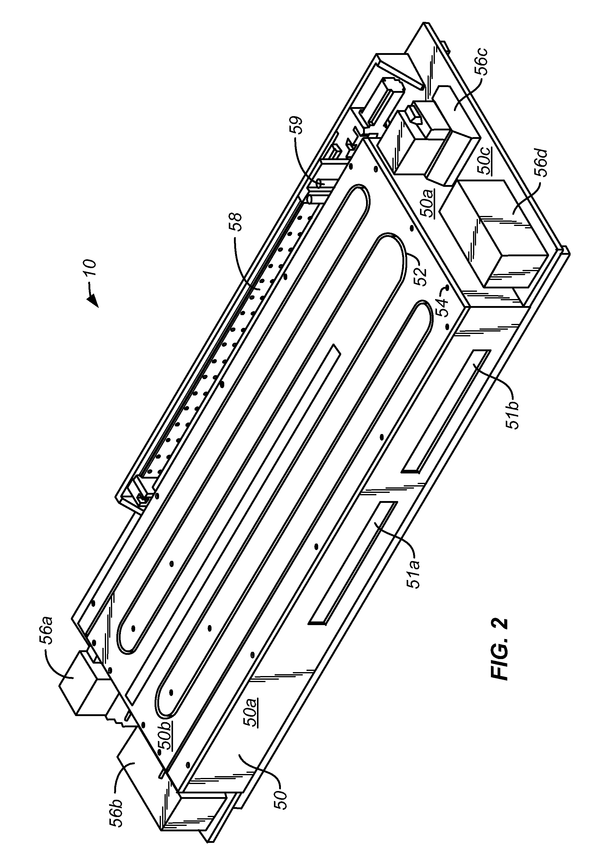
[0030]According to the present invention, techniques related to the field of semiconductor processing equipment are provided. More particularly, the present invention relates to a method and apparatus for measuring thermal characteristics of semiconductor processing apparatus. Merely by way of example, the method, apparatus and devices of the present invention are used to measure bake plate temperatures using thermal sensors that extend along heating elements of the bake plate. The method and apparatus can be applied to other processes for semiconductor substrates including other processing chambers.

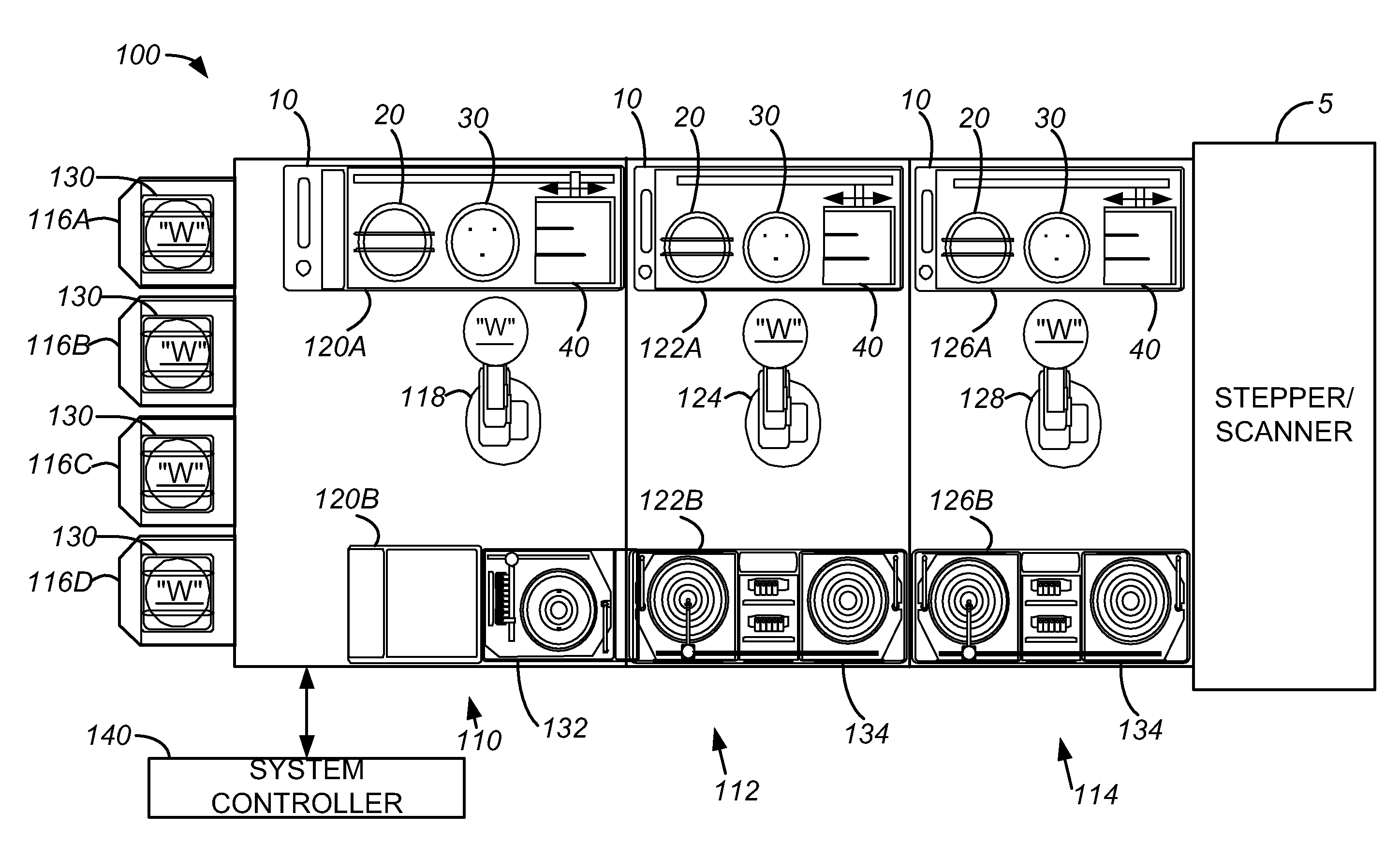
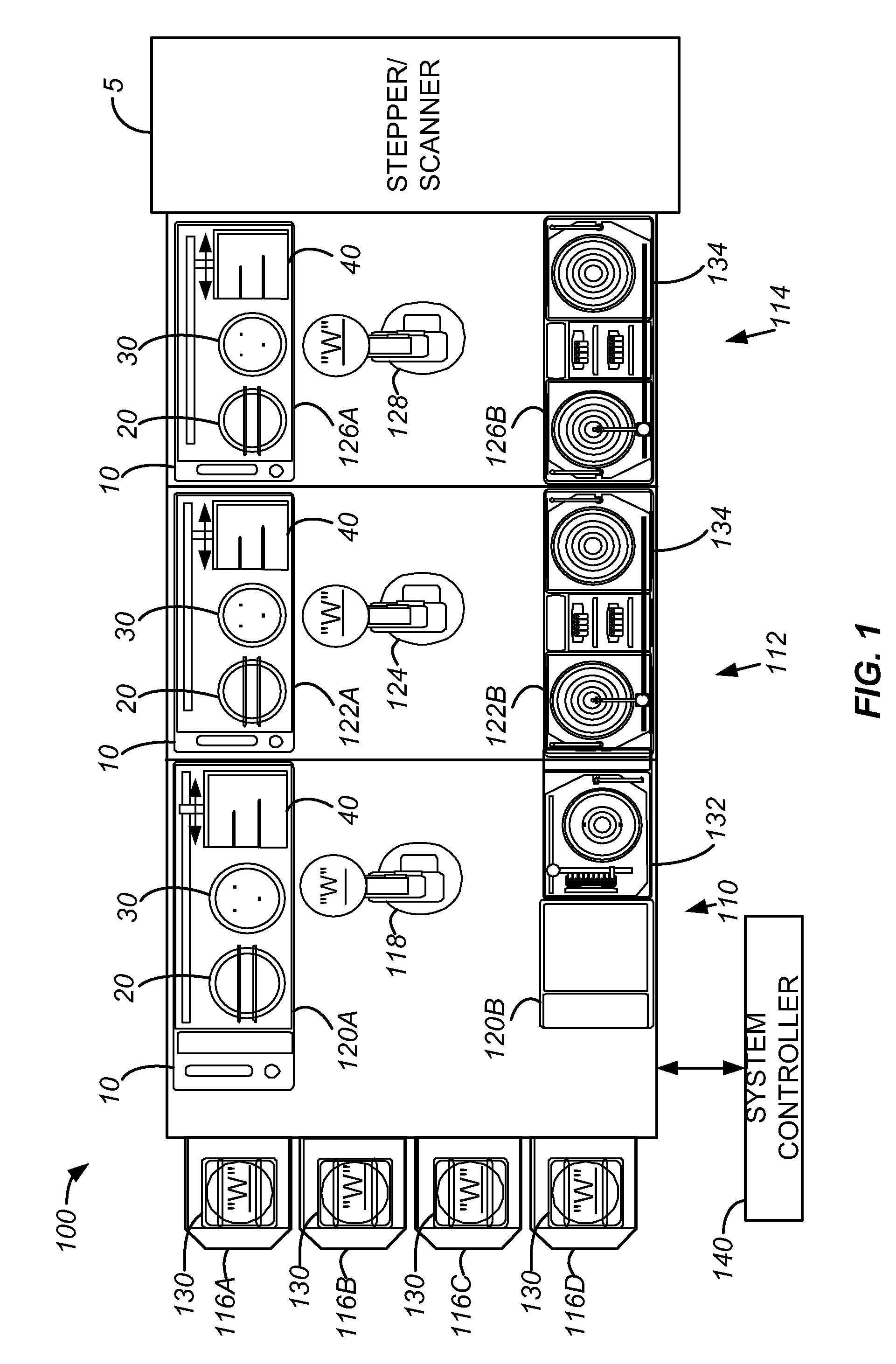
[0031]FIG. 1 is a plan view of one embodiment of a track lithography tool 100 in which the embodiments of the present invention may be used. As illustrated in FIG. 1, a cluster tool, for example track lithography tool 100, contains a front end module 110 (sometimes referred to as a factory interface), a central module 112, and a rear module 114 (sometimes referred to as a scanner interfa...


PUM


Abstract

A device for heating a semiconductor wafer comprises a heating element arranged to conduct heat toward the wafer. The heating element can extend along a heating element path. An RTD sensor loop can extend along an RTD sensor path. The RTD sensor path can be positioned along the heating element path to measure a temperature that corresponds to the heating element. The RTD sensor loop can measure an average temperature along the heating element. Portions of the RTD sensor can be interlaced between portions of the heating element. The heating element path can be arranged with interstices between portions of the heating element path, and portions of the RTD sensor path can be positioned within the interstices to interlace the RTD sensor loop with the heating element. The RTD sensor loop can comprise a soft metal that is resistant to oxidation and extends along the RTD sensor path.

Description

BACKGROUND OF THE INVENTION[0001]The present invention relates generally to the field of substrate processing equipment. More particularly, the present invention relates to a method, apparatus and devices for measuring thermal characteristics of semiconductor processing apparatus. Merely by way of example, the method and apparatus of the present invention are used to measure bake plate temperatures using thermal sensors that extend along heating elements of the bake plate. The method and apparatus can be applied to other processes for semiconductor substrates including other processing chambers.[0002]Modern integrated circuits contain millions of individual elements that are formed by patterning the materials, such as silicon, metal and dielectric layers, that make up the integrated circuit to sizes that are small fractions of a micrometer. The technique used throughout the industry for forming such patterns is photolithography. A typical photolithography process sequence generally ...

Claims


Application Information

Patent Timeline
IPC IPC(8): H01C7/02
CPCG01K1/14H01L21/67248H01L21/67103
Inventor VELLORE, KIM R.HERCHEN, HARALDLUE, BRIAN C.
Owner SOKUDO CO LTD
Why Eureka
Try Eureka