Electronic component, mounted structure, and inverter device therewith

a technology of mounted structure and inverter device, which is applied in the direction of fixed capacitor details, final product manufacturing, fixed capacitors, etc., can solve the problems of large effort, time, cost, etc., for mounting capacitors at a desired position on the circuit board, and it is difficult to automatize the mounting process, so as to improve withstanding voltage performance, prevent the occurrence of migration, and ensure the effect of withstanding voltag

Active Publication Date: 2008-09-18
TDK CORPARATION
View PDF8 Cites 1 Cited by
  • Summary
  • Abstract
  • Description
  • Claims
  • Application Information

AI Technical Summary

Benefits of technology

[0016]Preferably, the first lead conductor has a second portion laid on the first principal face so as to electrically connect the first portion of the first lead conductor to the first electrode; the second lead conductor has a second portion laid on the second principal face so as to electrically connect the first portion of the second lead conductor to the second electrode; the electronic component further comprises a first insulating film having at least a portion laid on the first principal face so as to cover the first electrode and the second portion of the first lead conductor, and a portion laid on the second principal face so as to cover the second electrode and the second portion of the second lead conductor. In this case, when the first portion of the first lead wire is soldered to the first portion of the first lead conductor and the first portion of the second lead wire is soldered to the first portion of the second lead conductor, the first insulating film makes it unlikely that solder attaching to the first portions of the first lead conductor and the second lead conductor will flow over the first side face and the second side face onto the first principal face and the second principal face. As a result, it becomes feasible to maintain the flat condition of the region corresponding to the first principal face and the region corresponding to the second principal face in the exterior of the electronic component.
[0017]More preferably, the electronic component further comprises a second insulating film being thermally resistant and laid so as to cover the element body, the first insulating film, the first portion of the first lead conductor, the first portion of the second lead conductor, the first portion of the first lead wire, and the first portion of the second lead wire. In this case, contact portions become closely fitted between the second insulating film and the element body and, when the armor is formed so as to further cover the second insulating film, the armor is closely fitted to the second insulating film. For this reason, even if heat is applied from the outside (e.g., when heat is applied during mounting the electronic component onto a circuit board by reflow soldering), the second insulating film becomes unlikely to peel off the element body and the armor becomes unlikely to peel off the second insulating film. As a result, it becomes feasible to ensure satisfactory withstanding voltage performance and to prevent occurrence of migration.
[0018]Preferably, the first lead conductor has a second portion laid on the first principal face so as to be drawn out from the first electrode and up to the first portion of the first lead conductor; the second lead conductor has a second portion laid on the second principal face so as to be drawn out from the second electrode and up to the first portion of the second lead conductor; the second portion of the first lead conductor and the second portion of the second lead conductor do not face each other when seen from a facing direction of the first principal face and the second principal face; and a position where the second portion of the second lead conductor is drawn out from the second electrode is set at a maximum direct distance from a position where the second portion of the first lead conductor is drawn out from the first electrode. In this case, the spacing becomes large between the first lead conductor and the second lead conductor. As a result, the dielectric breakdown voltage becomes larger and the withstanding voltage can be improved.
[0019]Preferably, the element body has a third side face and a fourth side face extending so as to couple the first principal face and the second principal face to each other, and facing each other; the first lead conductor has a second portion laid on the first principal face so as to be drawn out from the first electrode and up to the first portion of the first lead conductor; the second lead conductor has a second portion laid on the second principal face so as to be drawn out from the second electrode and up to the first portion of the second lead conductor; the second portion of the first lead conductor and the second portion of the second lead conductor do no face each other when seen from a facing direction of the first principal face and the second principal face; the second portion of the first lead portion extends from the first electrode toward the third side face; and the second portion of the second lead portion extends from the second electrode toward the fourth side face. In this case, the spacing becomes much larger between the first lead conductor and the second lead conductor As a result, the dielectric breakdown voltage becomes much greater and the withstanding voltage can be further improved.
[0020]Preferably, the element body is provided with a depression and / or a projection in a region between the first electrode and the second side face on the first principal face and in a region between the second electrode and the first side face on the second principal face. In this case, the creeping distance between the first electrode and the first portion of the second lead conductor and the creeping distance between the second electrode and the first portion of the first lead conductor become larger As a result, the dielectric breakdown voltage becomes larger and the withstanding voltage can be improved.
[0021]Preferably, the first electrode and the second electrode are of a round shape. If the first electrode and the second electrode have corners, an electric field will be likely to locally concentrate at the corners. When the first electrode and the second electrode are of the round shape, occurrence of the foregoing electric field concentration is suppressed. As a result, the dielectric breakdown voltage becomes larger and the withstanding voltage can be improved.

Problems solved by technology

It is, however, the present status that, for example, when the conventional capacitor as described in the foregoing application Laid-open No. 2-92916 is mounted onto the circuit board, a man manually performs, with each capacitor, a step of putting a distal end of each lead wire of the capacitor on a pad on the circuit board and soldering the distal end of the lead wire to the circuit board, which posed a problem of very large effort, time, cost, etc. for mounting of the capacitor.
For this reason, no flat face was present in the conventional capacitor and thus, when the conventional capacitor was attempted to be surface-mounted, the capacitor was so unsteady as to cause positional deviation during the mounting step thereof on the circuit board, resulting in failure in mounting the capacitor at a desired position on the circuit board.
In addition, since the conventional capacitor had no flat face, when it was attempted to be surface-mounted using a mounting apparatus for surface mounting of electronic component, it was hard for a suction nozzle of the mounting apparatus to suck the capacitor and it was difficult to automatize the mounting.

Method used


Image

  • Electronic component, mounted structure, and inverter device therewith
  • Electronic component, mounted structure, and inverter device therewith
  • Electronic component, mounted structure, and inverter device therewith

Examples


first embodiment

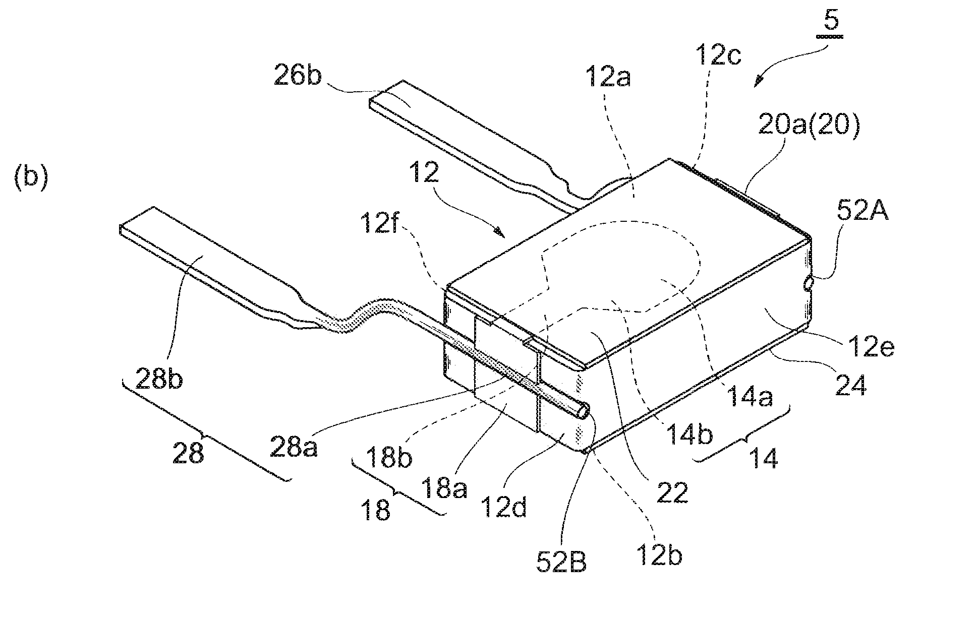
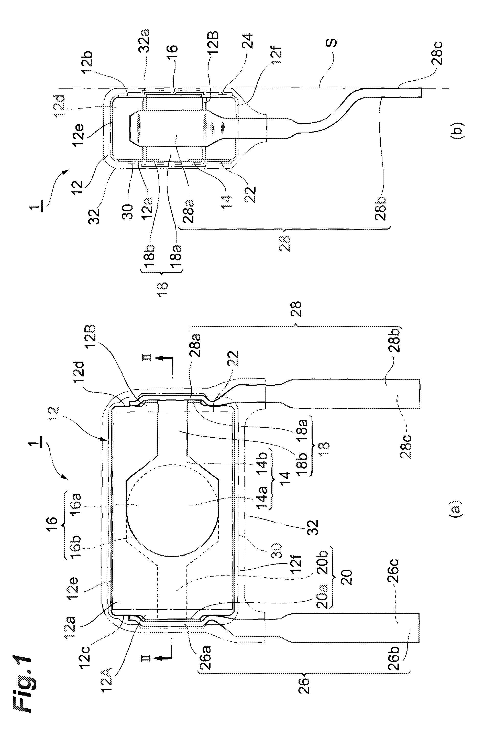
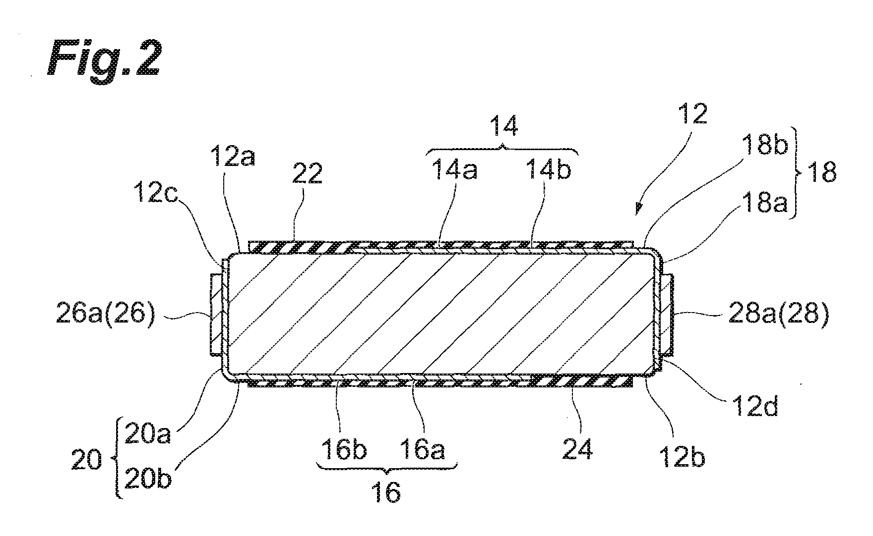
[0036]First, a structure of a surface mount type electronic component 1 according to the first embodiment will be described with reference to FIGS. 1 and 2. (a) of FIG. 1 is a perspective view of the surface mount type electronic component of the first embodiment from the principal face side of a dielectric element body and (b) of FIG. 1 a perspective view of the surface mount type electronic component of the first embodiment from the side face side of the dielectric element body. FIG. 2 is a sectional view along line II-II in (a) of FIG. 1. The surface mount type electronic component 1 of the first embodiment is an application of the present invention to a surface mount type capacitor.

[0037]The surface mount type electronic component 1, as shown in FIG. 1, has a dielectric element body (element body with a dielectric property) 12, electrodes 14, 16, lead conductors 18, 20, solder resists 22, 24, a pair of lead wires 26, 28, an undercoat 30, and an armor 32.

[0038]The dielectric elem...

second embodiment

[0076]The surface mount type electronic component 2 according to the second embodiment will be described below with reference to FIG. 6. (a) of FIG. 6 is a perspective view of the surface mount type electronic component of the second embodiment from the principal face side of the dielectric element body and (b) of FIG. 6 a sectional view along line VIb-VIb in (a) of FIG. 6. The surface mount type electronic component 2 of the second embodiment will be described below with focus on differences from the surface mount type electronic component 1 of the first embodiment, without redundant description.

[0077]The surface mount type electronic component 2, as shown in FIG. 6, has a dielectric element body 12, electrodes 14, 16, lead conductors 18, 20, solder resists 22, 24, a pair of lead wires 26, 28, an undercoat 30, and an armor 32.

[0078]The dielectric element body 12 has principal faces 12a, 12b facing each other, side faces 12c, 12d facing each other, and side faces 12e, 12f facing eac...


PUM


Abstract

There are provided an electronic component permitting easy surface mounting onto a circuit board and, a mounted structure and an inverter device therewith.
A surface mount type electronic component has a dielectric element body, electrodes, lead conductors, and lead wires. The dielectric element body has principal faces and side faces. One electrode is formed on one principal face, the other electrode is formed on the other principal face, and the electrodes face each other. A first portion of one lead conductor is laid on one side face. A first portion of the other lead conductor is laid on another side face. First portions of the lead wires are connected to the corresponding first portions of the lead conductors.

Description

BACKGROUND OF THE INVENTION[0001]1. Field of the Invention[0002]The present invention relates to an electronic component and, a mounted structure and an inverter device therewith.[0003]2. Related Background Art[0004]A conventionally known capacitor is constructed with an element body of a nearly circular cylinder shape having a pair of principal faces facing each other, a pair of electrodes formed on the respective principal faces of the element body, and a pair of lead wires connected to the respective electrodes (e.g., cf. Japanese Utility Model Application Laid-open No. 2-92916).SUMMARY OF THE INVENTION [0005]Presently, liquid crystal panels are used in a wide range of application, e.g., in liquid crystal displays, liquid crystal televisions, and so on. The liquid crystal panels are rapidly becoming larger and larger in these years and in conjunction therewith, the number of cold-cathode tubes used as backlights of the liquid crystal panel is also increasing. These cold-cathode t...

Claims


Application Information

Patent Timeline
Patent Type & Authority Applications(United States)
IPC IPC(8): H01G4/224
CPCH01C1/14H01G2/06H01G4/228H01G9/008H05K2201/10818H05K3/3426H05K2201/10462H05K2201/10651H05K1/181Y02P70/50
Inventor SHIRAKAWA, YUKIHIKOMIURA, IWAO
Owner TDK CORPARATION
Why Eureka
Try Eureka