Semiconductor device and method of forming the same

a semiconductor and semiconductor technology, applied in semiconductor devices, semiconductor/solid-state device details, electrical apparatus, etc., can solve the problems of increasing the leakage of p-n junction current, generating vacancy-type defects in the source and drain diffusion layer, and shortening the data retention time of the dram, so as to achieve the stability in energy, the effect of increasing the covalent radius and obtaining the stability in energy

Active Publication Date: 2008-09-25
HEFEI RELIANCE MEMORY LTD
View PDF9 Cites 14 Cited by
  • Summary
  • Abstract
  • Description
  • Claims
  • Application Information

AI Technical Summary

Benefits of technology

[0052]In some cases, the diffusion barrier layer may be a silicon film that contains at least one kind of element that is greater in covalent radius than silicon. In other cases, the diffusion barrier layer may be a silicon film that contains an excess amount of silicon. Once silicon atom at a lattice is replaced by the element greater in covalent radius than silicon, the element provides compressive strain to silicon lattices adjacent to the replaced element. Silicon vacancy provides tensile strain to silicon lattices adjacent to the silicon-vacancy. The polycrystal silicon film containing element as impurity, which is greater in covalent radius than silicon, is likely to capture silicon-vacancies while releasing silicon-interstitial, thereby obtaining the stability in energy.
[0053]The polycrystal silicon film containing an excess amount of silicon is likely to capture silicon-vacancies while releasing silicon-interstitial, thereby obtaining the stability in energy.
[0054]At least one of the polycrystal silicon film containing element as impurity, which is greater in covalent radius than silicon, and the polycrystal silicon film containing an excess amount of silicon, can be used as a diffusion barrier layer that separates the polycrystal silicon conductor or contact plug from the

Problems solved by technology

Silicon-interstitial in the source and drain diffusion layers are absorbed into the polycrystal silicon film that contacts with the source and drain diffusion layers, thereby generating vacancy-type defects in the source and drain diffusion layers.
The presence of vacancy-type defects in a depletion layer can increase the leakage of p-n junction current.
Increasing the leakage of p-n junction current shor

Method used


Image

  • Semiconductor device and method of forming the same
  • Semiconductor device and method of forming the same
  • Semiconductor device and method of forming the same

Examples


first embodiment

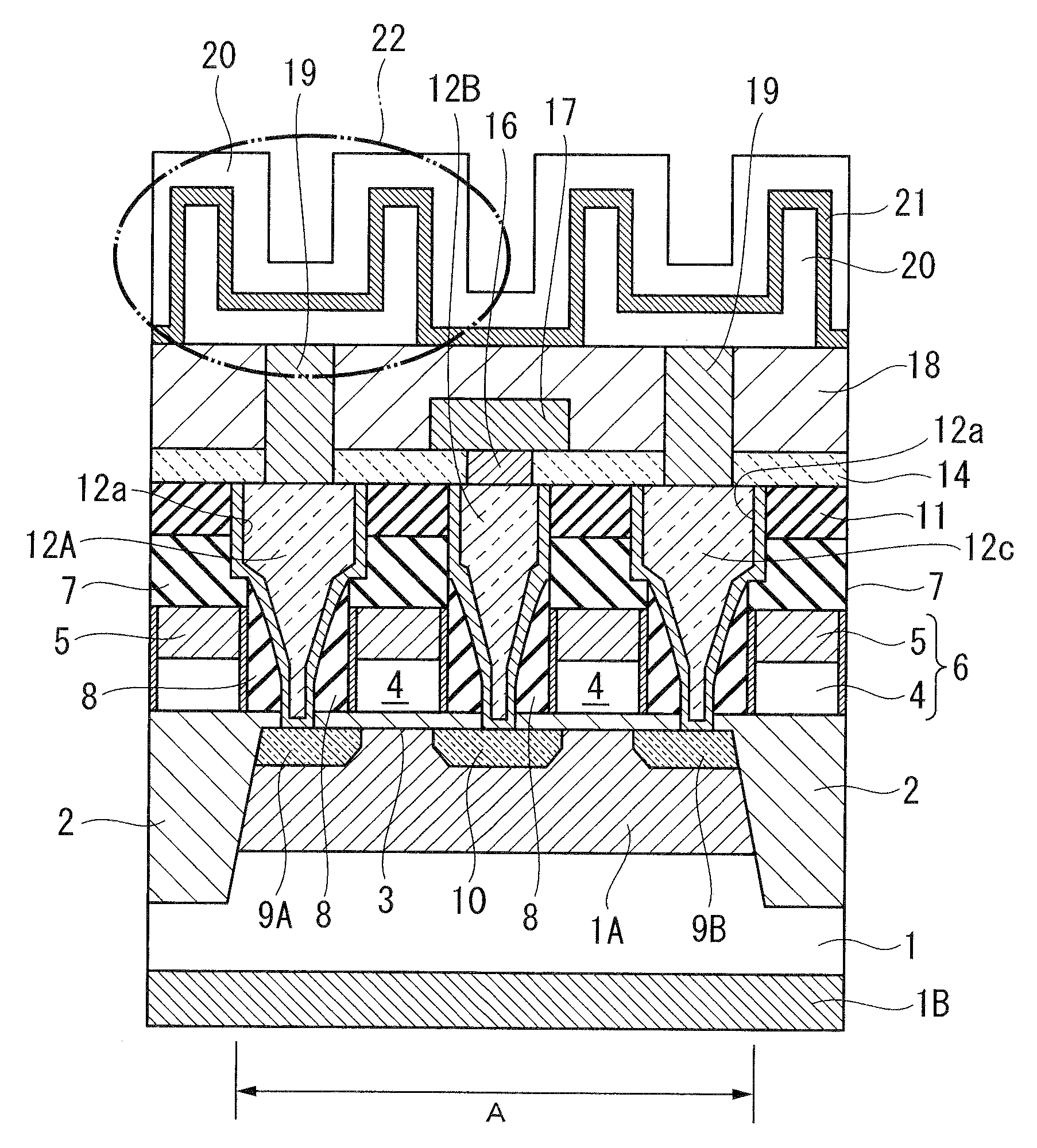
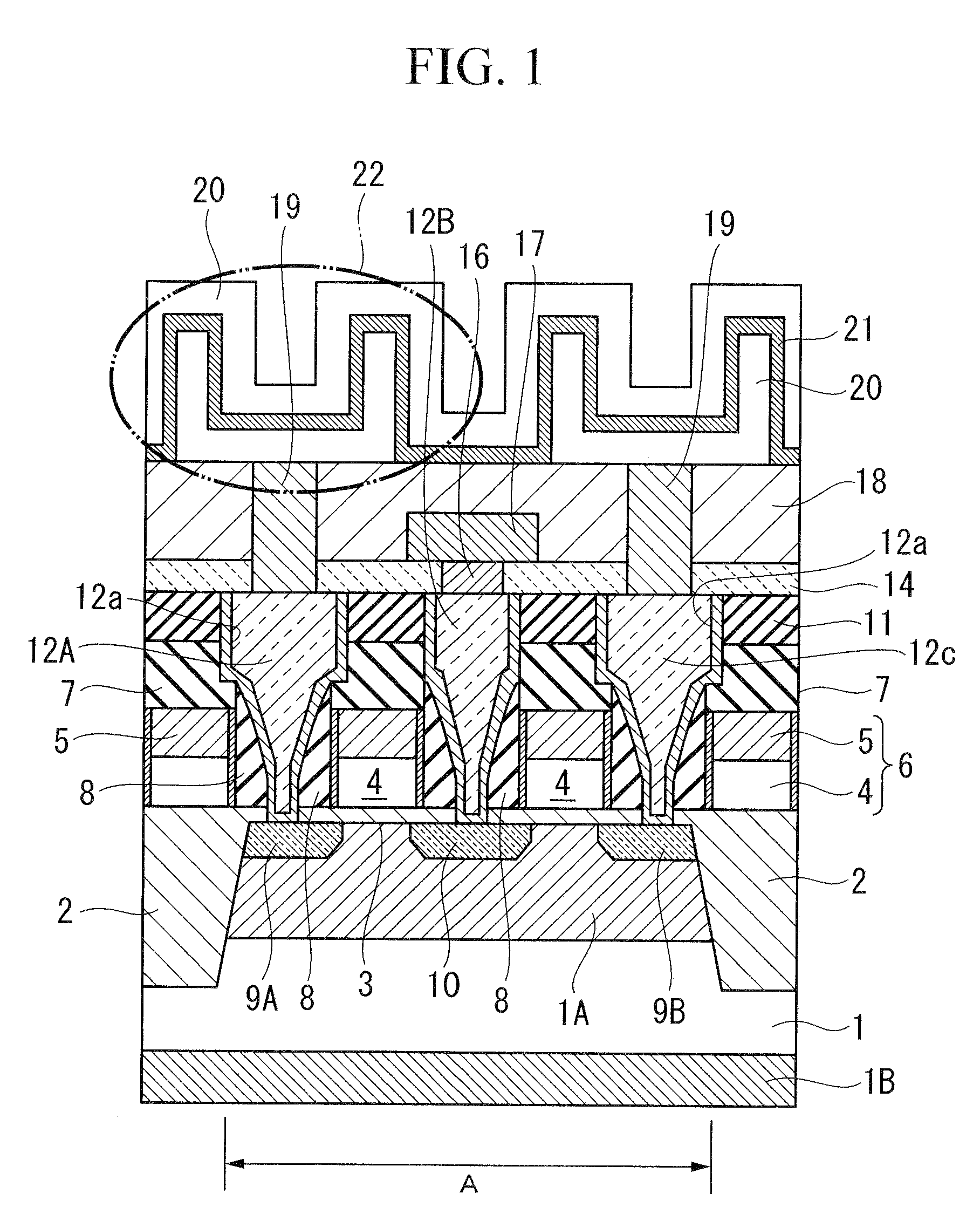
[0087]FIG. 1 is a fragmentary cross sectional elevation view illustrating a semiconductor device in accordance with the present invention. A semiconductor device is formed on a semiconductor substrate 1. In some cases, the semiconductor substrate 1 may be made of a semiconductor that contains impurity at a predetermined impurity concentration. Typically, the semiconductor substrate 1 may be made of silicon. A device isolation region 2 is selectively formed on the semiconductor substrate 1. The device isolation region 2 defines an active region A of the semiconductor substrate 1. The device isolation region 2 can be formed by a shallow trench isolation method. The device isolation region 2 isolates a selecting transistor or transistors which are formed in the active region A. The active region A is a region for forming a transistor or transistors. The active region A is defined by the device isolation region 2. A doped layer 1A is formed in a shallow region of the active region A.

[00...

second embodiment

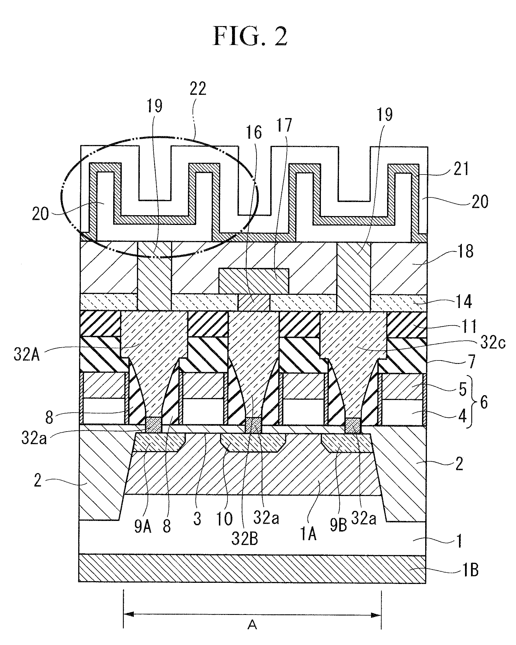
[0116]In accordance with the second embodiment, the semiconductor device of FIG. 2 has contact plugs 32A, 32B and 3C with diffusion barrier layers 32a. The diffusion barrier layer 12a covers only the bottom of each of the contact plugs 32A, 32B and 3C. The diffusion barrier layer 32a does not cover the side wall of each of the contact plugs 32A, 32B and 3C. Contact holes are formed in the gate insulating film 3, the side wall insulating film 8, the insulating film 7 and the first inter-layer insulator 11. Parts of the source and drain diffusion layers 9A, 9B and 10 are shown through the contact holes. The diffusion barrier layers 32a are provided at the bottoms of the contact holes. The diffusion barrier layers 32a contact with the source and drain diffusion layers 9A, 9B and 10. The diffusion barrier layers 32a fill the bottom portions of the contact holes. The contact plugs 32A, 32B and 3C are provided on the diffusion barrier layers 32a. The contact plugs 32A, 32B and 3C with the...


PUM


Abstract

A semiconductor device may include, but is not limited to, a single crystal silicon diffusion layer, a polycrystal silicon conductor, and a diffusion barrier layer. The diffusion barrier layer separates the polycrystal silicon conductor from the single crystal silicon diffusion layer. The diffusion barrier layer prevents a diffusion of at least one of silicon-interstitial and silicon-vacancy between the single crystal silicon diffusion layer and the polycrystal silicon conductor.

Description

BACKGROUND OF THE INVENTION[0001]1. Field of the Invention[0002]The present invention generally relates to a semiconductor device and a method of forming the same. More specifically, the present invention relates to a semiconductor device including a transistor that has source and drain diffusion layers, and polysilicon contact plugs that connect the source and drain diffusion layers to interconnections. Further specifically, the present invention relates to a semiconductor device which includes reduced defects that reside in one or more diffusion layers and reduced junction leakage of current.[0003]Priority is claimed on Japanese Patent Application No. 2006-259610, filed Sep. 25, 2006, the content of which is incorporated herein by reference.[0004]2. Description of the Related Art[0005]All patents, patent applications, patent publications, scientific articles, and the like, which will hereinafter be cited or identified in the present application, will hereby be incorporated by refe...

Claims


Application Information

Patent Timeline
IPC IPC(8): H01L29/78H01L23/52H01L21/4763
CPCH01L21/26506H01L21/28525H01L21/76843H01L21/76859H01L23/53271H01L2924/0002H01L29/66628H01L29/7834H01L2924/00H01L21/26513
Inventor OKONOGI, KENSUKEOHYU, KIYONORI
Owner HEFEI RELIANCE MEMORY LTD
Why Eureka
Try Eureka