Semiconductor device and manufacturing method of the same

Inactive Publication Date: 2008-09-25
RENESAS ELECTRONICS CORP
View PDF5 Cites 9 Cited by
  • Summary
  • Abstract
  • Description
  • Claims
  • Application Information

AI Technical Summary

Benefits of technology

[0018]The effect obtained by representative inventions among the inventions is briefly desc

Problems solved by technology

However, an insulating film with an excellent embeddability tends to become more hygroscopic (more likely to absorb moisture) compa

Method used


Image

  • Semiconductor device and manufacturing method of the same
  • Semiconductor device and manufacturing method of the same
  • Semiconductor device and manufacturing method of the same

Examples


first embodiment

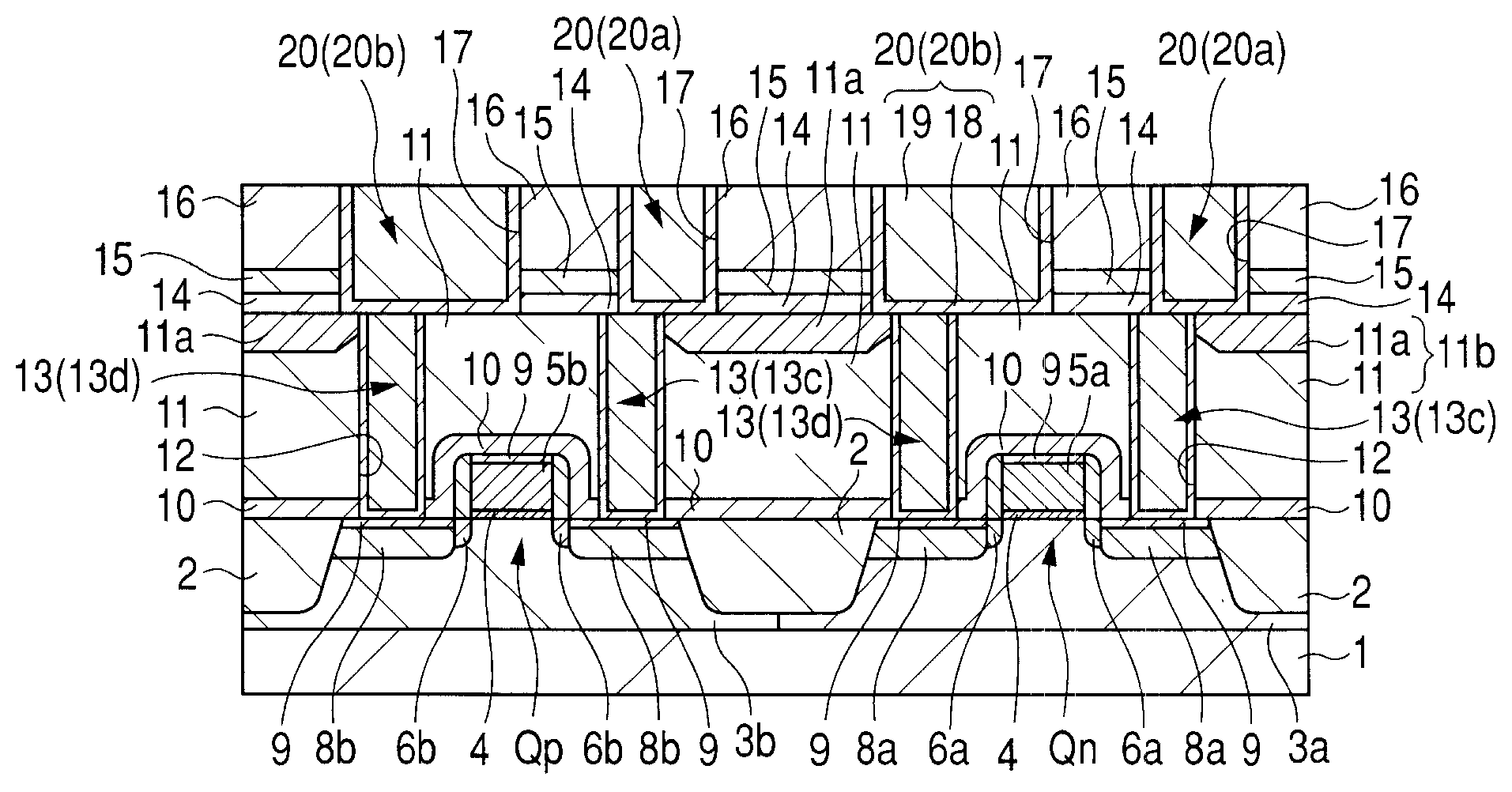
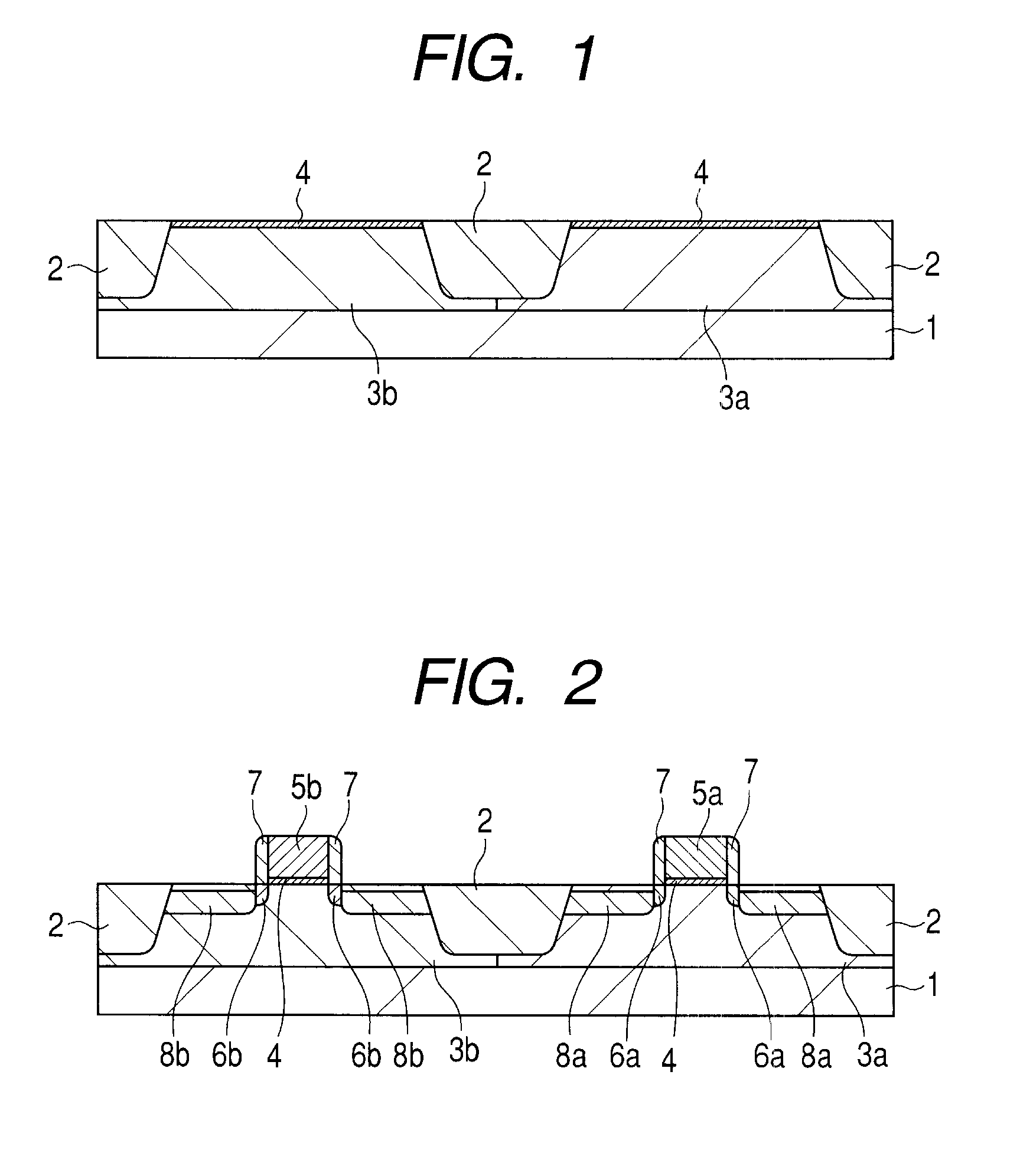
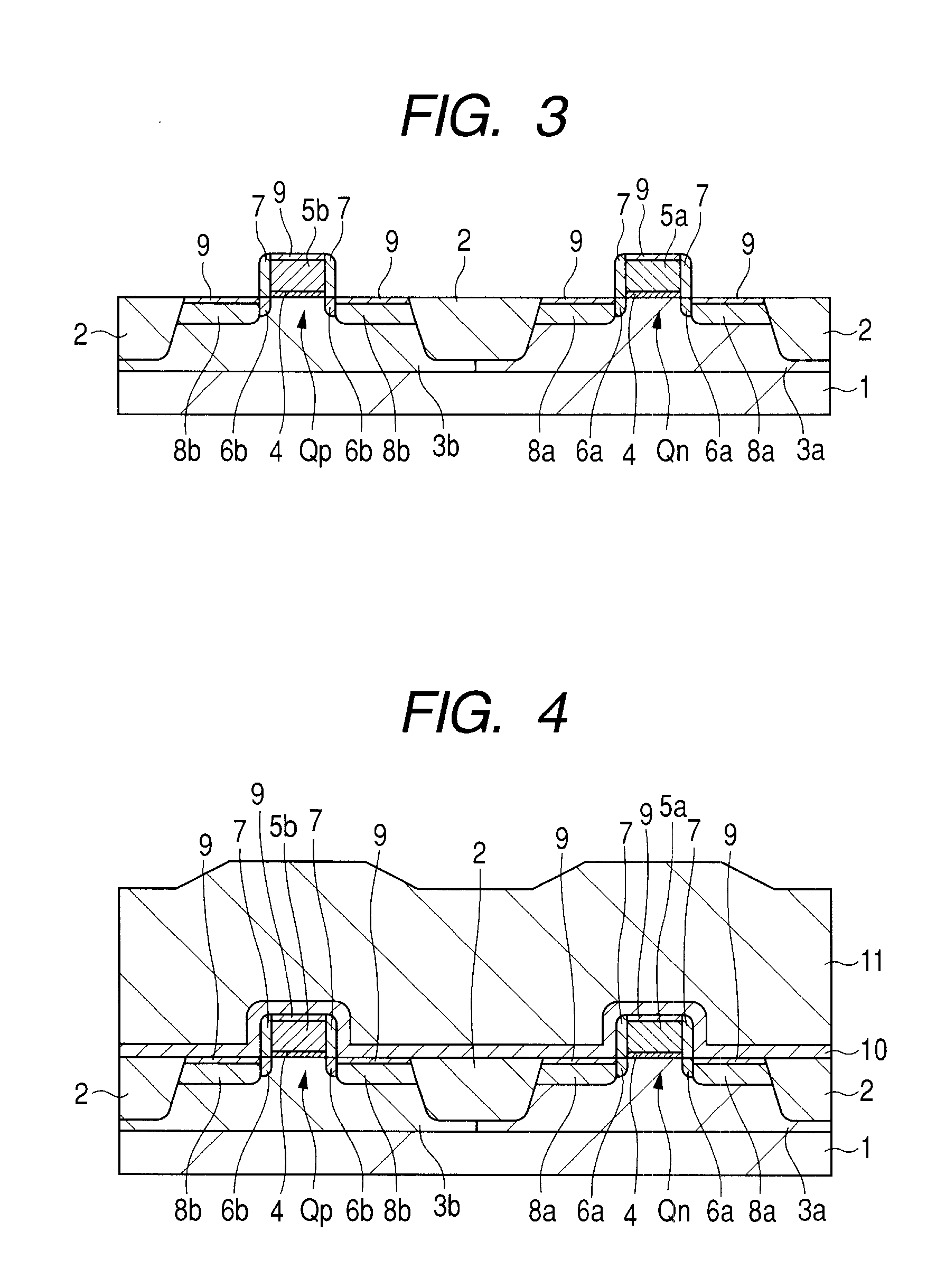
[0046]Semiconductor devices according to the preferred embodiments and their manufacturing process will be described with reference to the drawings. FIG. 1 to FIG. 14 are sectional views of essential parts in the manufacturing process of a semiconductor device according to an embodiment, for example, a semiconductor device having a MISFET (Metal Insulator Semiconductor Field Effect Transistor).

[0047]In order to manufacture a semiconductor device according to the present embodiment, first, a semiconductor substrate (semiconductor wafer) 1 including a p-type single crystal silicon etc. having a specific resistance of about, for example, 1 to 10 Ω·cm is prepared. Then, an element isolation region 2 is formed in the main surface of the semiconductor substrate 1. The element isolation region 2 includes silicon oxide etc. and can be formed by, for example, the STI (Shallow Trench Isolation) method or the LOCOS (Local Oxidization of Silicon) method.

[0048]Next, a p-type well 3a is formed in...

second embodiment

[0146]FIG. 19 to FIG. 23 are cross-sectional views of essential parts in a manufacturing process of a semiconductor device according to the present embodiment. The processes up to that in FIG. 4 are substantially the same as those in the first embodiment described above, and therefore, their description is omitted here and subsequent processes that follow that in FIG. 4 are described.

[0147]After substantially the same structure as that in FIG. 4 is obtained by carrying out the processes up to the film forming process of the insulating film 11 in the same manner as that in the first embodiment, in the present embodiment, an insulating film 11a (sixth insulating film) 11a is formed over the insulating film (first insulating film) 11, as shown in FIG. 19. The insulating film 11a includes a silicon oxide film formed by the plasma CVD method. Since the gap between gate electrodes 5a, 5b is filled with the insulating film 11, no problem about embeddability will arise even if the insulatin...


PUM


Abstract

The reliability of a semiconductor device having an embedded wire in the lowest layer wire is improved. In a main surface of a semiconductor substrate, MISFETs are formed and over the main surface, insulating films 10, 11 are formed. In the insulating films 10, 11 a contact hole is formed and a plug is embedded therein. Over the insulating film 11 in which the plug is embedded, insulating films 14, 15, 16 are formed and an opening is formed in the insulating films 14, 15, 16 and a wire is embedded therein. The insulating film 15 is an etching stopper film when etching the insulating film 16 in order to form the opening, containing silicon and carbon. The insulating film 11 has a high hygroscopicity and the insulating film 15 has a low moisture resistance, however, by interposing the insulating film 14 therebetween and making the insulating film 14 have a higher density of the number of Si (silicon) atoms than that of the insulating film 11, an electrically weak interface is prevented from being formed.

Description

CROSS-REFERENCE TO RELATED APPLICATION[0001]The present application claims priority from Japanese patent application No. 2007-74266 filed on Mar. 22, 2007, the content of which is hereby incorporated by reference into this application.BACKGROUND OF THE INVENTION[0002]The present invention relates to a semiconductor device and a manufacturing technique of the same and more particularly to a technique that is useful for the semiconductor device having an embedded wire and manufacturing method of the same.[0003]Elements of a semiconductor device are coupled by, for example, a multilayer wire structure to form circuits. As miniaturization advances, an embedded wire structure has been developed as a wire structure. An embedded wire structure is formed by, for example, embedding a wire material in a wire opening, such as wire groove or hole formed in an insulating film, using the Damascene technique (Single-Damascene technique and Dual-Damascene technique).[0004]In Japanese patent laid-op...

Claims


Application Information

Patent Timeline
IPC IPC(8): H01L23/52H01L21/4763
CPCH01L21/76832H01L21/76883H01L21/76834H01L21/3205
Inventor FURUSAWA, TAKESHIKAMOSHIMA, TAKAOAMISHIRO, MASATSUGUSUZUMURA, NAOHITOFUKUI, SHOICHIOKADA, MASAKAZU
Owner RENESAS ELECTRONICS CORP
Why Eureka
Try Eureka