Clock Signal Generation Device, Semiconductor Integrated Circuit, and Data Reproduction Method

a clock signal and clock signal technology, applied in the field of clock signal generation devices, semiconductor integrated circuits, and data reproduction methods, can solve the problems of reducing the time required for clock signal reproduction, affecting the quality of clock signal reproduction, and reducing the frequency error between the reproduced signal and the clock signal, so as to increase the capture range, stable clock signal, and the effect of reducing the time required

Inactive Publication Date: 2008-09-25
PANASONIC CORP
View PDF7 Cites 11 Cited by
  • Summary
  • Abstract
  • Description
  • Claims
  • Application Information

AI Technical Summary

Benefits of technology

[0050]By immediately determining a phase synchronization state of the reproduced signal and the clock signal based on the control signal output from the loop filter means, and by properly controlling the clock signal generation device, it is possible to generate a stable clock signal.
[0051]According to a clock signal generation device of the present invention, it is possible to enlarge a capture range by correcting a range where the phase error value can be calculated. As a result, it is possible to perform the resynchronization, even if the reproduced signal and the clock signal are not synchronous with each other due to the rapid change of the reproduced signal.
[0052]The gain of the loop filter means and the gain of the offset canceling means and phase error range determining means are controlled in accordance with the determination result on the range of the phase error values and the determination result on the synchronization state. In a case where the reproduced signal and the clock signal are not synchronous with each other, the gains are set to be high and a range where the phase error values can be calculated is enlarged. As a result, it is possible to quickly perform the lead-in operation into a synchronous state. In a case where the reproduced signal and the clock signal are synchronous with each other, the gains are set to be low and the range where phase error values can be calculated is not corrected. As a result, it is possible to generate a stable clock signal.
[0053]According to another clock signal generation device of the present invention, a distribution of displacements of the phase error values is obtained and a deviation of the distribution is detected. When the detected deviation is large, a control signal controlling the frequency of the clock signal is generated based on the phase error values such that the deviation of the distribution should be eliminated. As a result, it is possible to exactly detect a state where the PPL cannot capture the frequency error between the reproduced signal and the clock signal, even if the quality of the reproduced signal is bad. By controlling the frequency of the clock signal such that the frequency error is within the capture range according to the detection result, it is possible to generate a stable clock signal.
[0054]According to one embodiment of the present invention, a distribution of displacements of the phase error values is obtained with an accumulated value obtained by accumulating signs of the displacements of the phase error values. As a result, it is not necessary to hold many phase error values, and it is possible to realize a high precision detection using a small scale circuit.
[0055]According to one embodiment of the present invention, the amplitude of a short mark / space portion is amplified by the higher frequency band emphasizing means. As a result, it is possible to improve a precision in detecting a binary level and to stabilize the lead-in operation of the PLL.

Problems solved by technology

However, in a conventional technique, a range where the phase error value can be calculated is limited to only ±½ cycle of the clock signal.
Thus, in a case where the frequency error between the reproduced signal and the clock signal is increased rapidly, or in a case where the quality of the reproduced signal is degraded due to dust, scratches or finger prints on the optical disc, a state where the reproduced signal and the clock signal are not synchronous with each other may occur.
Once the reproduced signal and the clock signal are not synchronous with each other, a problem occurs in that it takes long time until the reproduced signal and the clock signal are synchronous with each other, and there is also a problem that, in the worst case, the reproduced signal and the clock signal are not expected to be synchronous with each other, so that data cannot be reproduced.
Accordingly, once the reproduced signal and the clock signal are not synchronous with each other when the quality of the reproduced signal is degraded due to dust, scratches or finger prints on the optical disc, there is problem that it takes long time until the reproduced signal and the clock signal are synchronous with each other, so that the reproduction performance is degraded.
Accordingly, in a case where the capture range of the PLL is narrow and the frequency of the reproduced signal differs from the frequency of the clock signal, it takes long time to perform the lead-in operation of the PLL.

Method used


Image

  • Clock Signal Generation Device, Semiconductor Integrated Circuit, and Data Reproduction Method
  • Clock Signal Generation Device, Semiconductor Integrated Circuit, and Data Reproduction Method
  • Clock Signal Generation Device, Semiconductor Integrated Circuit, and Data Reproduction Method

Examples


first embodiment

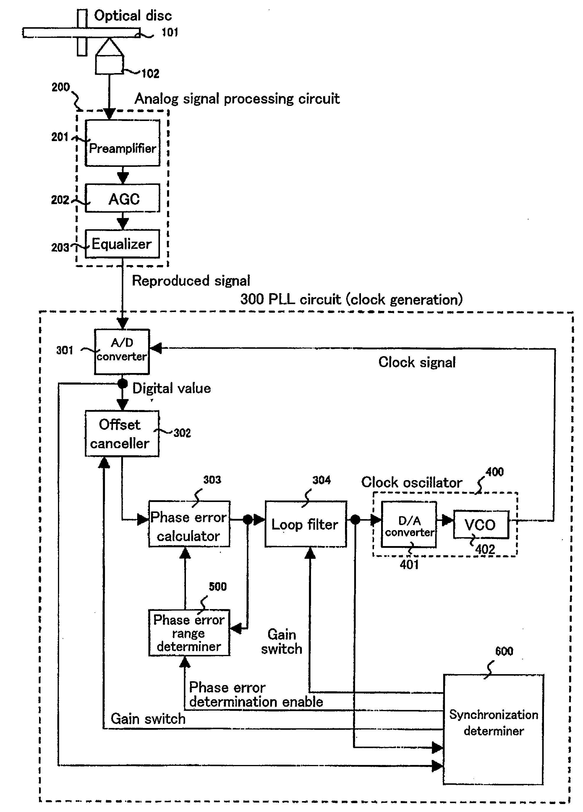
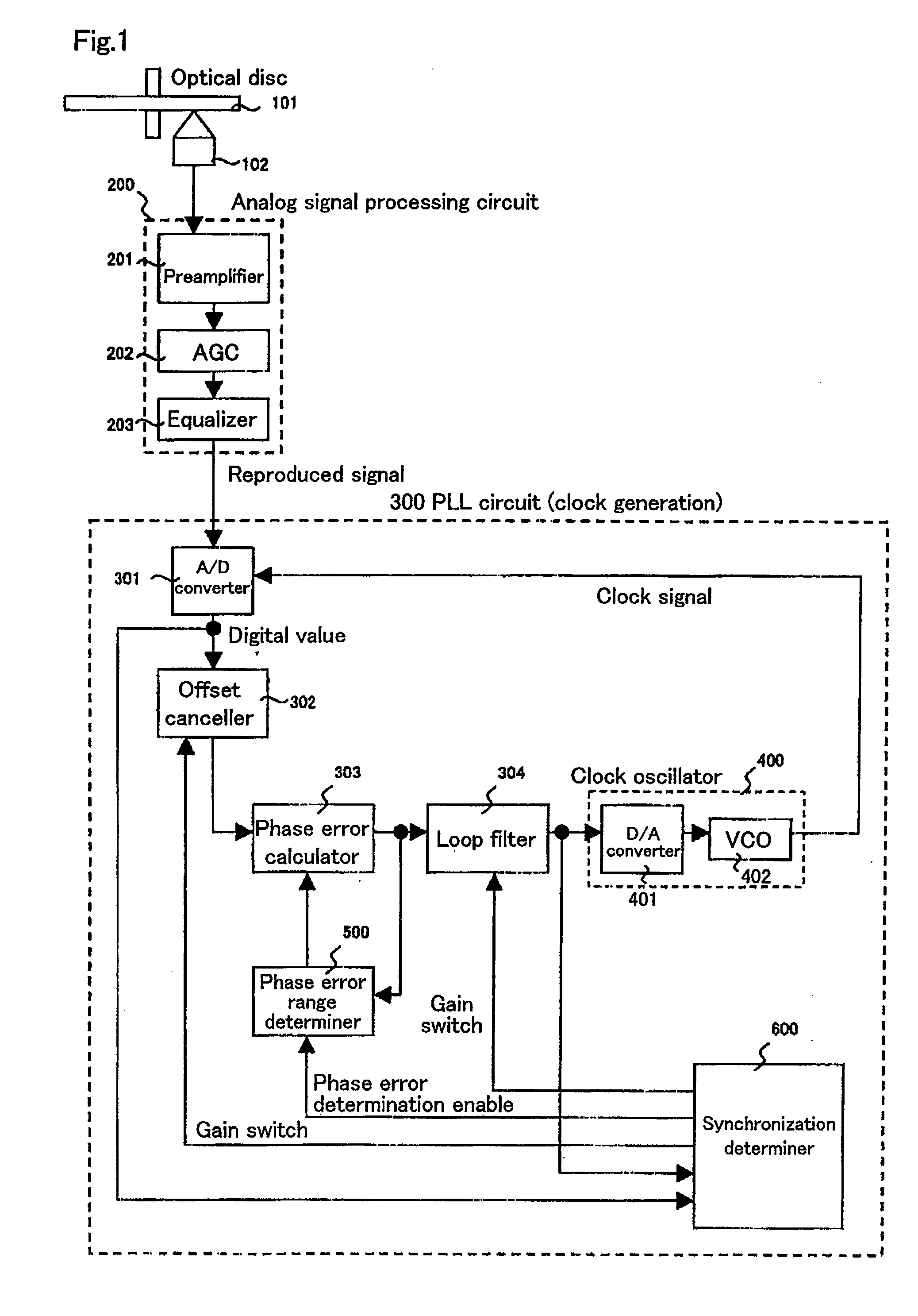
[0077]FIG. 1 is a block diagram showing a configuration of a PLL circuit in a first embodiment of the present invention.

[0078]An optical head 102 irradiates an optical disc 101 with a light beam, detects an amount of the reflected light from the optical disc 101 and outputs an electric signal. An analog signal processing circuit 200 extracts a reproduced signal from the electric signal output from the optical head 102. The analog signal processing circuit 200 includes a preamplifier 201 for amplifying the electric signal, a gain control circuit (AGC) 202 for controlling the amplitude of the amplified signal to be constant and an equalizer 203 improving a frequency characteristic.

[0079]Next, a configuration of a PLL circuit 300 will be described.

[0080]The PLL circuit 300 generates a clock signal which is synchronous with a reproduced signal. The clock signal generation circuit 300 includes: an A / D converter 301 for digitalizing the reproduced signal with the clock signal; an offset c...

second embodiment

[0118]FIG. 9 is a block diagram showing a configuration of a clock signal generation circuit in a second embodiment of the present invention.

[0119]The clock signal generation device shown in FIG. 9 generates a clock signal using an optical disc 1101 on which information is recorded. The clock signal generation device includes: an optical head 1102; an analog signal processing circuit 1200; and a clock signal generation circuit 1300.

[0120]The optical head 1102 irradiates the optical disc 1101 with a light beam 1102a, detects an amount of the reflected light from the optical disc 1101 and generates an electric signal 1102b based on the amount of the reflected light.

[0121]The analog signal processing circuit 1200 extracts a reproduced signal 1200a from the electric signal 1102b. The analog signal processing circuit 1200 includes: a preamplifier 1201 for amplifying the electric signal 1102b; a gain control circuit (AGC) 1202 for controlling the amplitude of the amplified signal to be co...

third embodiment

[0161]FIG. 16 is a block diagram showing a configuration of the clock signal generation circuit in a third embodiment of the present invention. In FIG. 16, the same reference numerals are given to the elements which are the same as those shown in FIG. 9, and the descriptions of those elements will be omitted.

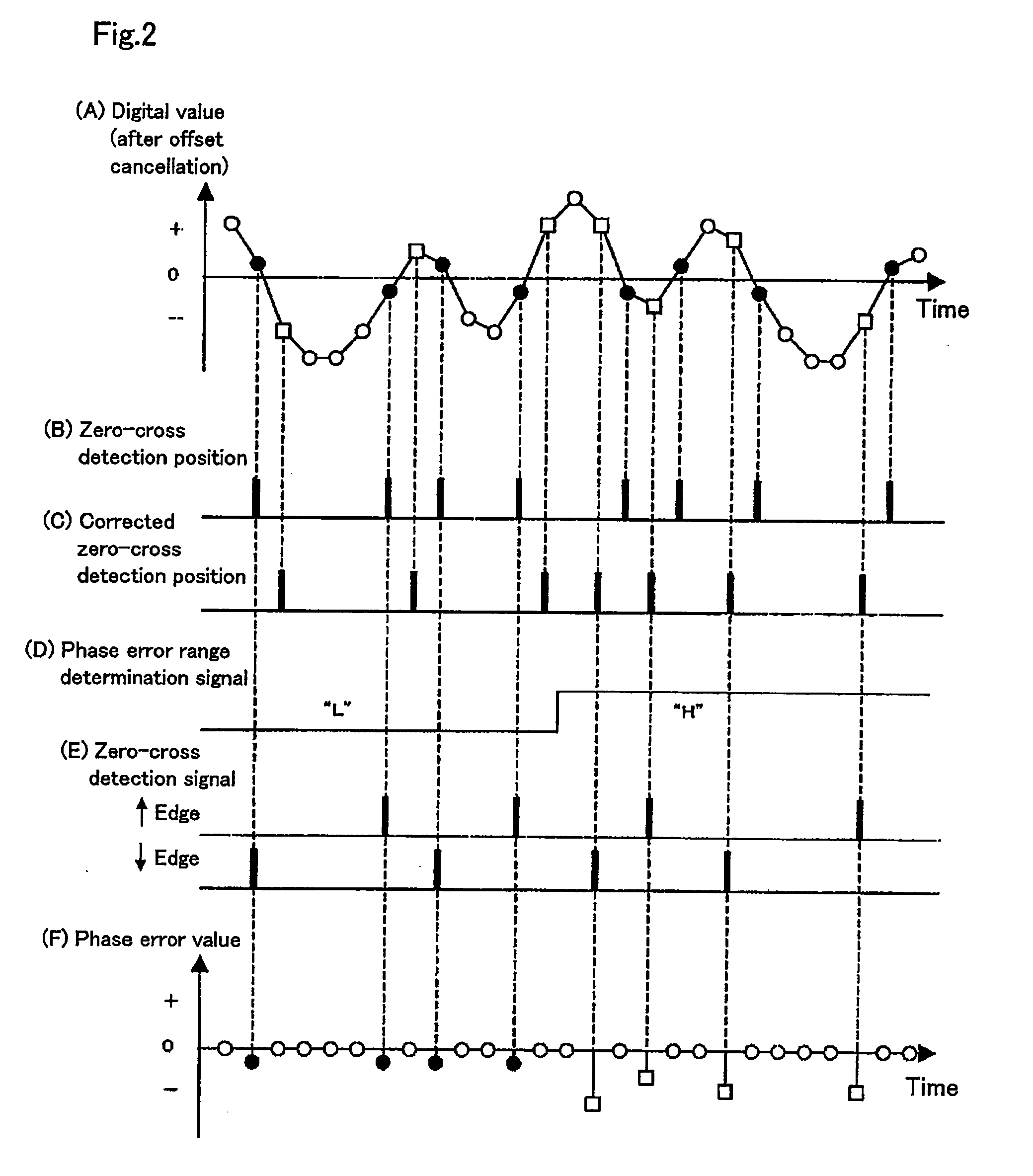
[0162]The offset canceller 1302 is controlled such that a center level of the digital value 1301a output from the A / D converter 1301 becomes zero. The offset canceller 1302 includes: a zero level detector 3021; binary DUTY detector 3022; an accumulator 3023, a subtracter 3025; and a higher frequency band emphasizing filter 3024.

[0163]The higher frequency band emphasizing filter 3024 outputs a higher frequency band emphasizing filter output value 3024a which is obtained by emphasizing a higher frequency band component of the digital value 1302a after the offset cancellation. For example, a short mark, such as 2T or 3T where the amplitude can be easily reduced, or a short space po...


PUM

PropertyMeasurementUnit
phase erroraaaaaaaaaa
phaseaaaaaaaaaa
frequencyaaaaaaaaaa

Abstract

The present invention improves a lead-in time of the PLL with a phase error detector having an enlarged range of phase error detection and gain control based on the PLL synchronous state. The phase error detection range is enlarged by correcting the phase error detection point in a case where the phase error increases. A locked state of the PLL is determined based on a standard deviation of the smoothed phase error values and the gains are switched between a lead-in transient state and a stationary state. As a result, it is possible to shorten and stabilize the lead-in time of the PLL.

Description

TECHNICAL FIELD[0001]The present invention relates to a PLL device (clock signal generation device) for generating a timing signal (clock signal) for binarizing the reproduced signal reproduced from a medium on which information is recorded, a semiconductor integrated circuit used therein and a data reproduction method.BACKGROUND ART[0002]Conventionally, when information is reproduced from an optical disc on which the information is recorded, a signal reproduced from the disc is input to a PLL (Phase Locked Loop) circuit, a clock signal which is synchronous with the reproduced signal is generated by the PLL circuit, and the reproduced signal is digitalized in synchronization with the clock signal so as to reproduce digital data (see, for example, Reference 1 below).[0003]FIG. 19 is a block diagram showing a configuration of a conventional PLL circuit for generating a clock signal.[0004]An optical head 4102 irradiates an optical disc 4101 with a light beam, detects an amount of the r...

Claims


Application Information

Patent Timeline
Patent Type & Authority Applications(United States)
IPC IPC(8): H03L7/06G11B7/005G11B20/14H03L7/08H03L7/091H03L7/095H03L7/107
CPCG11B7/094G11B7/0941G11B20/1403H03M1/1255H03L7/107H03L7/1077H03L7/091H03L7/1075
Inventor NAKATA, KOHEIMIYASHITA, HARUMITSU
Owner PANASONIC CORP
Why Eureka
Try Eureka