Waveform shaping apparatus, optical transmission system, and waveform shaping method

a waveform shaping and optical transmission technology, applied in multiplex communication, instruments, semiconductor lasers, etc., can solve the problem that the waveform shaping technology cannot provide simultaneous waveform shaping for wdm signal beams

Active Publication Date: 2008-09-25
FUJITSU LTD
View PDF14 Cites 10 Cited by
  • Summary
  • Abstract
  • Description
  • Claims
  • Application Information

AI Technical Summary

Benefits of technology

[0010]It is an object of the present invention to at least partially solve the problems in the conventional technology.

Problems solved by technology

However, due to the underlining principle, the above-described waveform shaping technology cannot provide simultaneous waveform shaping for WDM signal beams.

Method used


Image

  • Waveform shaping apparatus, optical transmission system, and waveform shaping method
  • Waveform shaping apparatus, optical transmission system, and waveform shaping method
  • Waveform shaping apparatus, optical transmission system, and waveform shaping method

Examples


first embodiment

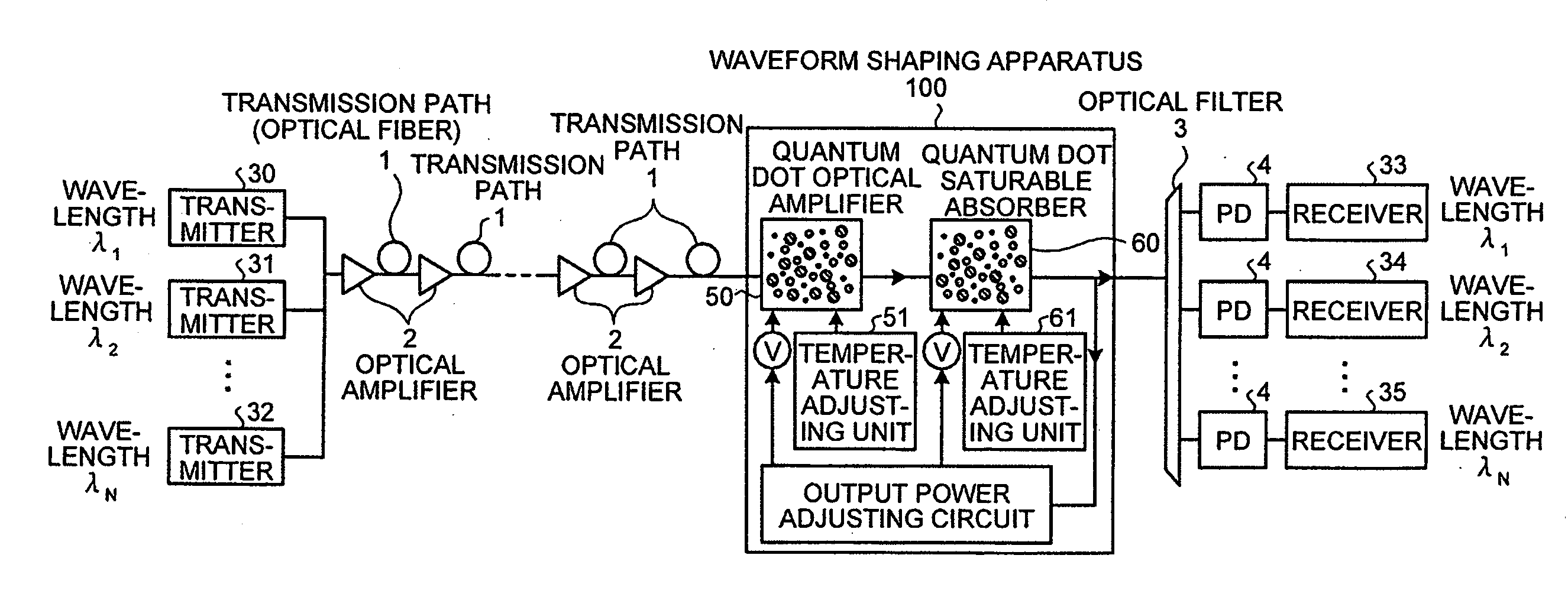
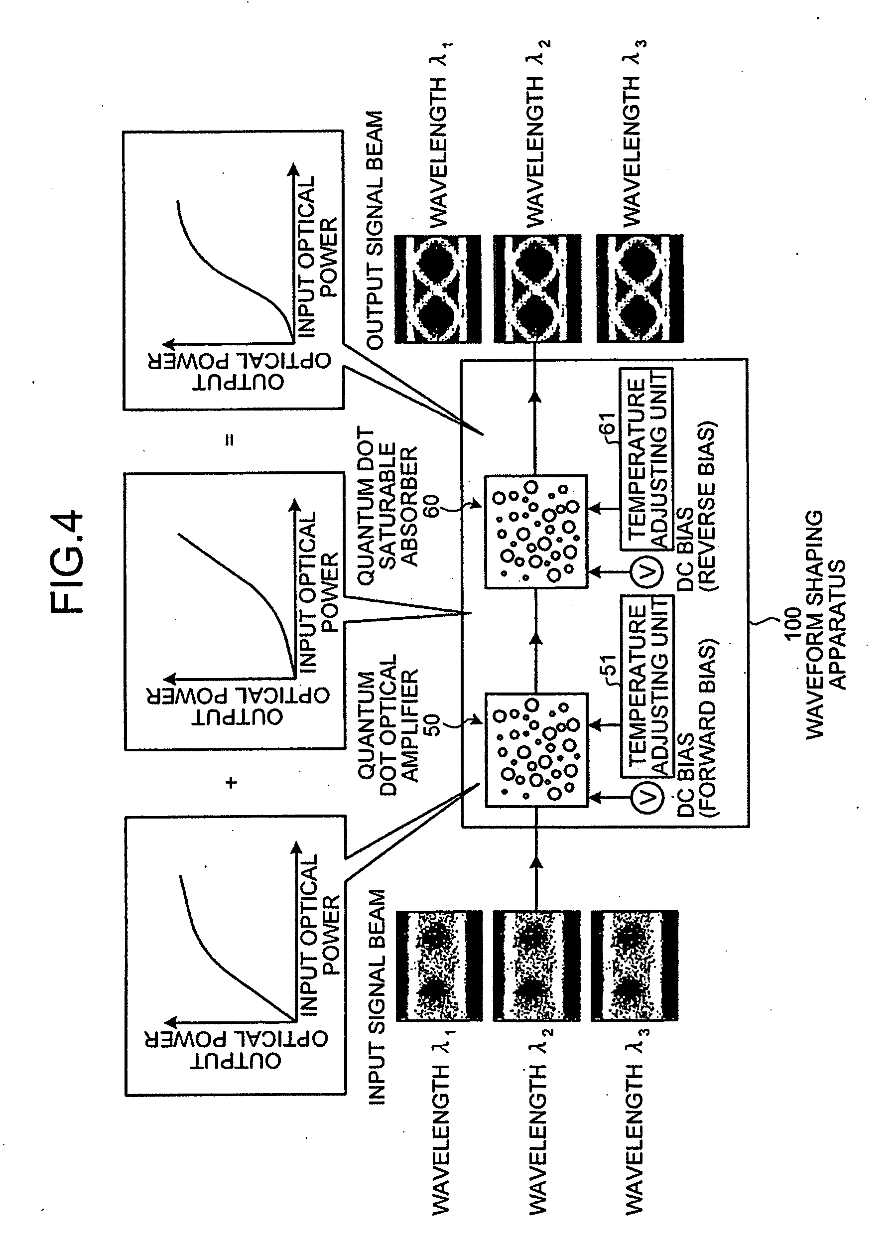
[0045]The waveform shaping apparatus can provide a simultaneous waveform shaping to the waveforms of the signal beams, each having a wavelength assigned to a channel, by allowing the signal beams to pass through the quantum dot optical amplifier and the quantum dot saturable absorber having quantum dots adjusted in size. In this manner, the entire system can be simplified.

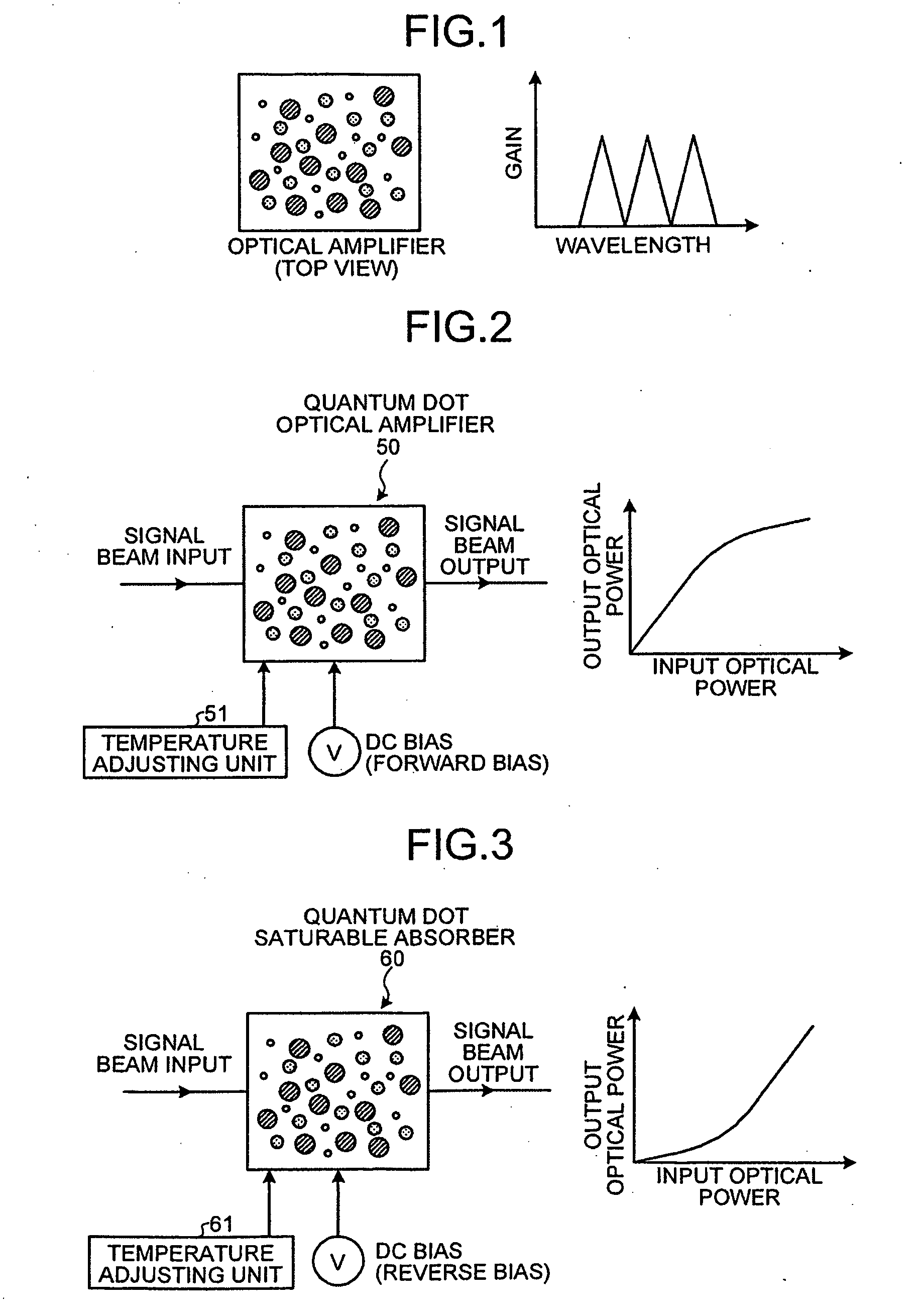
[0046]The optical amplifier that has the substrate with quantum dots layered thereon and amplifies a signal beam at an optical wavelength corresponding to the size of the quantum dots (hereinafter, referred simply to as “optical amplifier”) will be now explained. Instead of a generally available quantum well (QW) structure, the optical amplifier according to the first embodiment uses a structure of quantum dots of sizes between several nanometers to several tens of nanometers.

[0047]FIG. 1 is a schematic for explaining the optical amplifier according to the first embodiment. The schematic at the left in FIG. 1 is a...

second embodiment

[0075]The waveform shaping apparatus can adjust the power of each of the wavelengths of the signal beams by using the filter. Therefore, each of the wavelengths can be adjusted to the power most suitable for a quantum dot optical amplifier 210 and a quantum dot saturable absorber 220 that perform the waveform shaping of the signal beams.

[0076]A structure of the waveform shaping apparatus according to the second embodiment will be now explained. FIG. 8 is a schematic of a waveform shaping apparatus 200 according to the second embodiment. As shown in FIG. 8, the waveform shaping apparatus 200 includes the quantum dot optical amplifier 210, the quantum dot saturable absorber 220, and an equalizing filter 230.

[0077]The quantum dot optical amplifier 210 corresponds to the quantum dot optical amplifier 50 explained in FIG. 2, and the forward bias is applied to the quantum dot optical amplifier 210. The quantum dot optical amplifier 210 is maintained at a predetermined temperature set by ...

third embodiment

[0085]As described above, the waveform shaping apparatus monitors the signal beams output from the quantum dot optical amplifier and the quantum dot saturable absorber, and adjusts the forward bias and the reverse bias applied to the quantum dot optical amplifier and the quantum dot saturable absorber, respectively. Therefore, more precise waveform shaping can be provided to the signal beams.

[0086]A structure of the waveform shaping apparatus according to the third embodiment will be now explained. FIG. 10 is a schematic of a waveform shaping apparatus 250 according to the third embodiment. As shown in FIG. 10, the waveform shaping apparatus 250 includes a quantum dot optical amplifier 260, a quantum dot saturable absorber 270, temperature adjusting units 261 and 271, drivers 262 and 272, an equalizing filter 280, a directional coupler 281, a filter 282, and a monitor 283.

[0087]The quantum dot optical amplifier 260 corresponds to the quantum dot optical amplifier 50 explained in FI...


PUM

PropertyMeasurementUnit
sizeaaaaaaaaaa
poweraaaaaaaaaa
wavelengthaaaaaaaaaa

Abstract

A waveform shaping apparatus includes a quantum dot optical amplifier in which an amplification factor of input signal beams saturates if the optical power of the signal beams is equal to or greater than a predetermined value; and a quantum dot saturable absorber in which an absorption factor of the input signal beams saturates if the optical power of the signal beams is under a predetermined value. The quantum dot optical amplifier and the quantum dot saturable absorber are connected in series with a transmission path of the signal beams, and shape the waveform of the signal beams. Voltages applied to the quantum dot optical amplifier and the quantum dot saturable absorber, respectively, are adjusted based on the optical power of the signal beams.

Description

BACKGROUND OF THE INVENTION[0001]1. Field of the Invention[0002]The present invention relates to a waveform shaping apparatus that shapes a waveform of a signal beam, and more specifically, to a waveform shaping apparatus, an optical transmission system, and a waveform shaping method that can simultaneously shape waveforms of a plurality of signal beams each having a wavelength assigned to a channel.[0003]2. Description of the Related Art[0004]To prevent waveform degradation of a signal beam transmitted over an optical fiber, various waveform shaping technologies have been thought out and commercialized.[0005]One example of the waveform shaping technologies is disclosed in Japanese Patent Application Laid-open No. 2003-15097. FIG. 24 is a schematic for explaining a waveform shaping technology according to this disclosure. This document discloses a waveform shaping technology that shapes a waveform of a signal beam using two optical gates (OGs) (a first OG and a second OG).[0006]As s...

Claims


Application Information

Patent Timeline
Patent Type & Authority Applications(United States)
IPC IPC(8): H04B10/12G02F1/35
CPCB82Y20/00G02F1/3523G02F1/3556G02F2203/26H01S5/026H01S5/3412H04J14/0284H04B10/2507H04B10/299H04B2210/003H04J14/02H04J14/0221H01S5/50
Inventor FUTAMI, FUMIOWATANABE, SHIGEKI
Owner FUJITSU LTD
Why Eureka
Try Eureka