Transistor Device and Method of Manufacture Thereof

a technology of transistors and dielectric materials, applied in the direction of semiconductor devices, transistors, electrical apparatus, etc., can solve the problems of reducing the speed and performance of transistors having high k gate dielectric materials, reducing the threshold voltage vt, and reducing the mobility of transistors, so as to prevent the effect of polysilicon depletion and boron penetration effects when the device is operated in inversion mod

Inactive Publication Date: 2008-09-25
INFINEON TECH AG
View PDF99 Cites 65 Cited by
  • Summary
  • Abstract
  • Description
  • Claims
  • Application Information

AI Technical Summary

Benefits of technology

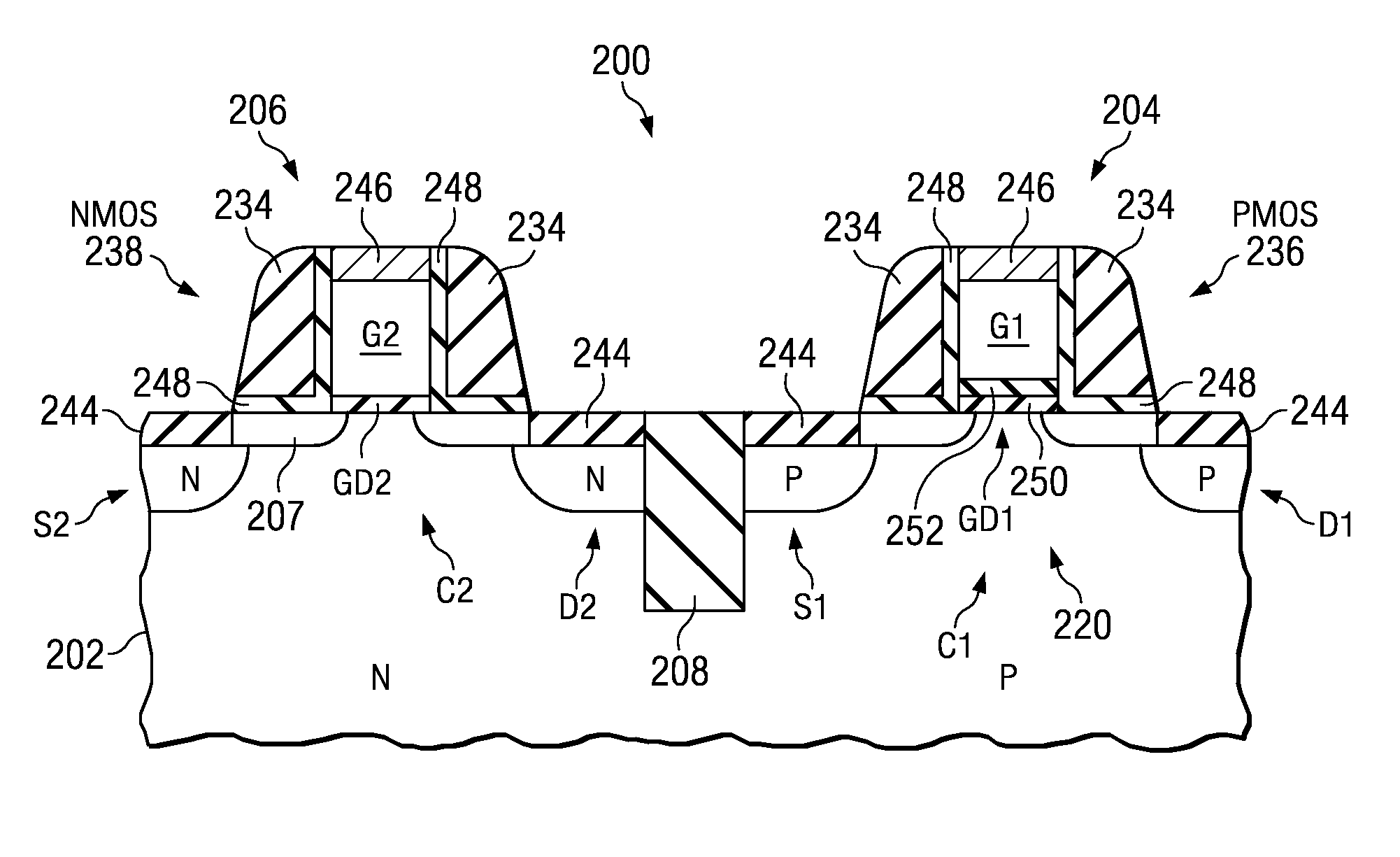
[0017]These and other problems are generally solved or circumvented, and technical advantages are generally achieved, by preferred embodiments of the present invention, which provide transistors and methods of manufacture thereof having a substantially symmetric threshold voltage Vt for the PMOS and NMOS transistors. The gate material of a PMOS transistor is doped with an n-type dopant, and the gate of an NMOS transistor is doped with a p-type dopant or n-type dopant, in a CMOS device. In some embodiments, a different gate dielectric material is used for the PMOS transistor than for the NMOS transistor. Polysilicon depletion effects are reduced or avoided by the novel embodiments of the present invention described herein.
[0022]Advantages of preferred embodiments of the present invention include providing a method of fabricating a CMOS device and structure thereof, wherein the PMOS transistor and NMOS transistor have a symmetric Vt. The threshold voltage Vt is decreased compared to prior art CMOS devices, and the flat band voltage is easier to tune. Embodiments of the invention may utilize high-k dielectric materials as the gate dielectric, using polysilicon, partially silicided, or fully silicided gate electrodes. Polysilicon depletion and boron penetration effects when the device is operated in an inversion mode are prevented, because the semiconductive material of the gates function in an accumulation regime, due to the presence of the novel reversal of dopants implanted in the PMOS and NMOS gates. The capacitance effective thickness (CET) of a CMOS device can be decreased in accordance with embodiments of the present invention.

Problems solved by technology

However, as devices are scaled down in size, using silicon dioxide for a gate dielectric becomes a problem because of gate leakage current, which can degrade device performance.
However, one problem with using high k materials as gate dielectric materials is lower mobility, which is undesirable.
Device performance using high k dielectric materials tends to suffer from trapped charge in the dielectric layer, which deteriorates the mobility, making the drive current lower than in transistors having silicon dioxide gate oxides, thus reducing the speed and performance of transistors having high k gate dielectric materials.
Another problem of using high k materials as a gate dielectric is that if polysilicon is used as a gate material in conjunction with a high k gate dielectric, poly (polysilicon) depletion can occur between the gate dielectric and the gate.
However, poly depletion decreases the capacitance and lowers the drive current of the CMOS device, which is undesirable.
Another problem with using a high-k dielectric material as the gate dielectric of a CMOS transistor is referred to in the art as a “Fermi-pinning” effect, which occurs at the interface of the gate electrode and gate dielectric material.
Fermi-pinning is a problem that occurs in CMOS devices having both polysilicon and metal gates.
The Fermi-pinning effect causes a threshold voltage shift and low mobility, due to the increased charge caused by the Fermi-pinning effect.
Fermi-pinning causes an assymmetric turn-on threshold voltage Vt for the two transistors of a CMOS device, which is undesirable.
Thus, a symmetric Vt for the NMOS and PMOS transistors of a CMOS device having a high k material for the gate dielectric cannot be achieved by doping polysilicon gate material, as in SiO2 gate dielectric CMOS devices.
Efforts have been made to improve the quality of high-k dielectric films and resolve the Fermi-pinning problems, but the efforts have resulted in little success.

Method used


Image

  • Transistor Device and Method of Manufacture Thereof
  • Transistor Device and Method of Manufacture Thereof
  • Transistor Device and Method of Manufacture Thereof

Examples


Embodiment Construction

[0033]The making and using of the presently preferred embodiments are discussed in detail below. It should be appreciated, however, that the present invention provides many applicable inventive concepts that can be embodied in a wide variety of specific contexts. The specific embodiments discussed are merely illustrative of specific ways to make and use the invention, and do not limit the scope of the invention.

[0034]High-k gate dielectrics generally yield orders of magnitude lower gate leakage current than SiO2 gate dielectrics with the same effective oxide thickness (EOT). For low standby power (LSTP) and high performance (HP) applications, the use of a high-k material for a gate dielectric is a potential solution in the roadmap for the advanced technology nodes. Using high-k materials for gate dielectrics in CMOS devices has resulted in good EOT, lower gate leakage (Jg), mobility and hysteresis parameters, but the devices suffer from lack of Vt controllability. In order to make h...


PUM


Abstract

A CMOS device includes high k gate dielectric materials. A PMOS device includes a gate that is implanted with an n-type dopant. The NMOS device may be doped with either an n-type or a p-type dopant. The work function of the CMOS device is set by the material selection of the gate dielectric materials. A polysilicon depletion effect is reduced or avoided.

Description

[0001]This application is a divisional of U.S. application Ser. No. 11 / 017,062, filed on Dec. 20, 2004, and entitled “Transistor Device and Method of Manufacture Thereof,” which application is hereby incorporated herein by reference.CROSS-REFERENCE TO RELATED APPLICATIONS[0002]This application relates to the following co-pending and commonly assigned patent application Ser. No. 10 / 870,616, filed on Jun. 17, 2004, and entitled “CMOS Transistor with Dual High-k Gate Dielectric and Method of Manufacture Thereof,” which application is hereby incorporated herein by reference.TECHNICAL FIELD[0003]The present invention relates generally to semiconductor devices, and more particularly structures for and methods of manufacturing transistors.BACKGROUND[0004]Semiconductor devices are used in a variety of electronic applications, such as personal computers, cell phones, digital cameras, and other electronic equipment, as examples. Semiconductor devices are typically fabricated by sequentially d...

Claims


Application Information

Patent Timeline
Patent Type & Authority Applications(United States)
IPC IPC(8): H01L21/8238
CPCH01L21/28194H01L21/823842H01L27/092H01L29/517H01L29/518H01L21/823857
Inventor LI, HONG-JYH
Owner INFINEON TECH AG
Why Eureka
Try Eureka