Organic Semiconductor Element and Organic El Display Device Using the Same

a technology of organic el and semiconductor elements, applied in the direction of solid-state devices, transistors, thermoelectric devices, etc., can solve the problems of unsatisfactory coverage and increase in contact resistance, and achieve the effect of increasing drain current, reducing contact resistance, and very accurate channel length control

Inactive Publication Date: 2008-10-02
ROHM CO LTD
View PDF1 Cites 12 Cited by
  • Summary
  • Abstract
  • Description
  • Claims
  • Application Information

AI Technical Summary

Benefits of technology

[0018]With the structure of the organic semiconductor element of the present invention, the channel region is formed on the side surface of the organic semiconductor layer or the portion of the organic semiconductor layer where the gate electrode near the side surface of the second conductive layer is opposed to the first conductive layer, and the channel length is determined by the thickness of the organic semiconductor layer. For this reason, the channel length can be controlled very accurately in nanometer order. Further, the organic semiconductor layer and the source / drain electrodes are formed into a flat laminated structure, so that the problem of coverage due to a step does not arise. As a result, the contact resistance reduces, and a FET having desired channel length can be formed into an accurate dimension. For this reason, transistor properties such as an increase in the drain current and a decrease in the operating voltage can be improved greatly.
[0019]Further, since the gate electrode is formed on an upper surface, in the case where, for example, one of the source / drain of the switching element is connected to the gate electrode of the driving element in the display device, or where a control circuit in which the capacitor is connected to the gate of the driving element, the circuit can be formed simply by laminating the layers on the upper surface sequentially. Particularly when this organic semiconductor layer is applied to the organic light emitting (EL) display device, the display device can be formed by laminating the organic semiconductor layer and the organic EL section (light emitting section).
[0020]As a result, while the organic semiconductor is being used, the semiconductor element having an FET with very short channel length can be obtained, and the channel length can be controlled by the thickness of the organic semiconductor layer. For this reason, the FET with very definite channel length in nanometer order can be formed without using the photolithography technique, and it can be used as the driving element of the organic light emitting (EL) display device. Further, the FET can be formed only by the simple laminated structure or the channel portion is formed in a self-consistent manner, the process cost can be reduced, and the FET can be obtained at the very low cost.
[0021]Further, due to the structure of the organic EL display device of the present invention, even when the driving element is not obtained by the photolithography technique, the FET with short channel length and very low contact resistance can be obtained. Further, the driving element and the capacitor can be formed on the organic EL section only by the simple laminated structure, and the driving element or the like does not have to be arranged in parallel with the display section, so that the most part of each pixel area can be formed by the organic EL section. As a result, the aperture can be improved very greatly, and the organic EL display device which can provide clear display can be obtained at the very low cost. Further, since the electric current flows to the vertical direction in the driving element having the vertical structure, the electric current flows continuously with the organic EL section. For this reason, no useless path is present and even when the electric current can be allowed to flow by the low resistance and the upper electrode of the organic EL section and the source / drain electrodes on the lower surface for the driving element are not provided, the electric current can be allowed to flow from the driving element to the organic EL section. As a result, the active-matrix type organic light emitting (EL) display device with high performance can be obtained at the low cost, thereby contributing to the new progress of image display devices.

Problems solved by technology

For this reason, its coverage is not satisfactory, so that the contact resistance rises.

Method used


Image

  • Organic Semiconductor Element and Organic El Display Device Using the Same
  • Organic Semiconductor Element and Organic El Display Device Using the Same
  • Organic Semiconductor Element and Organic El Display Device Using the Same

Examples


Embodiment Construction

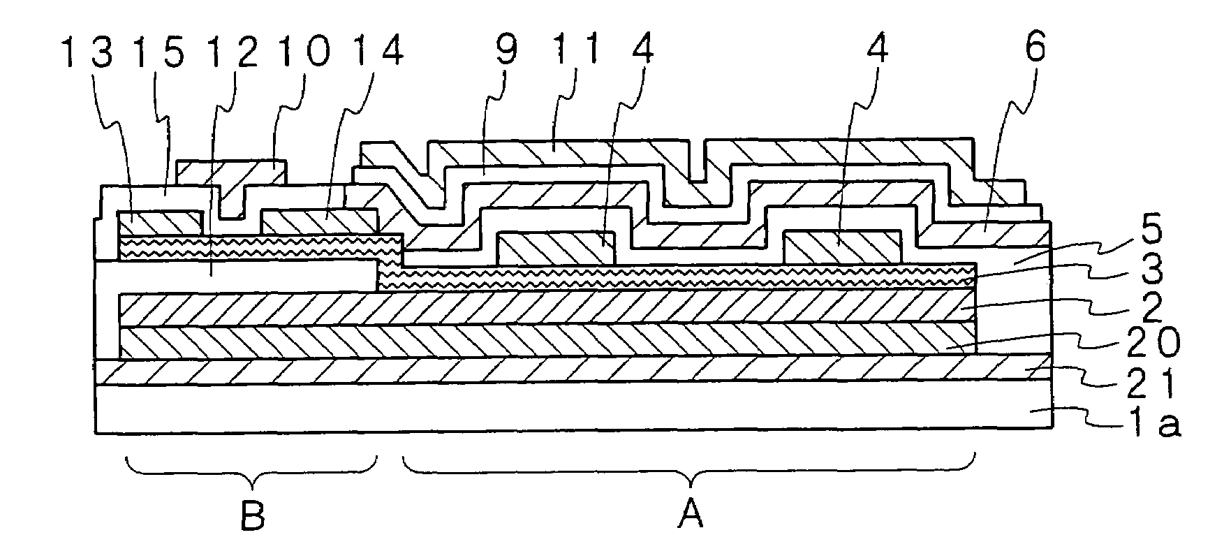
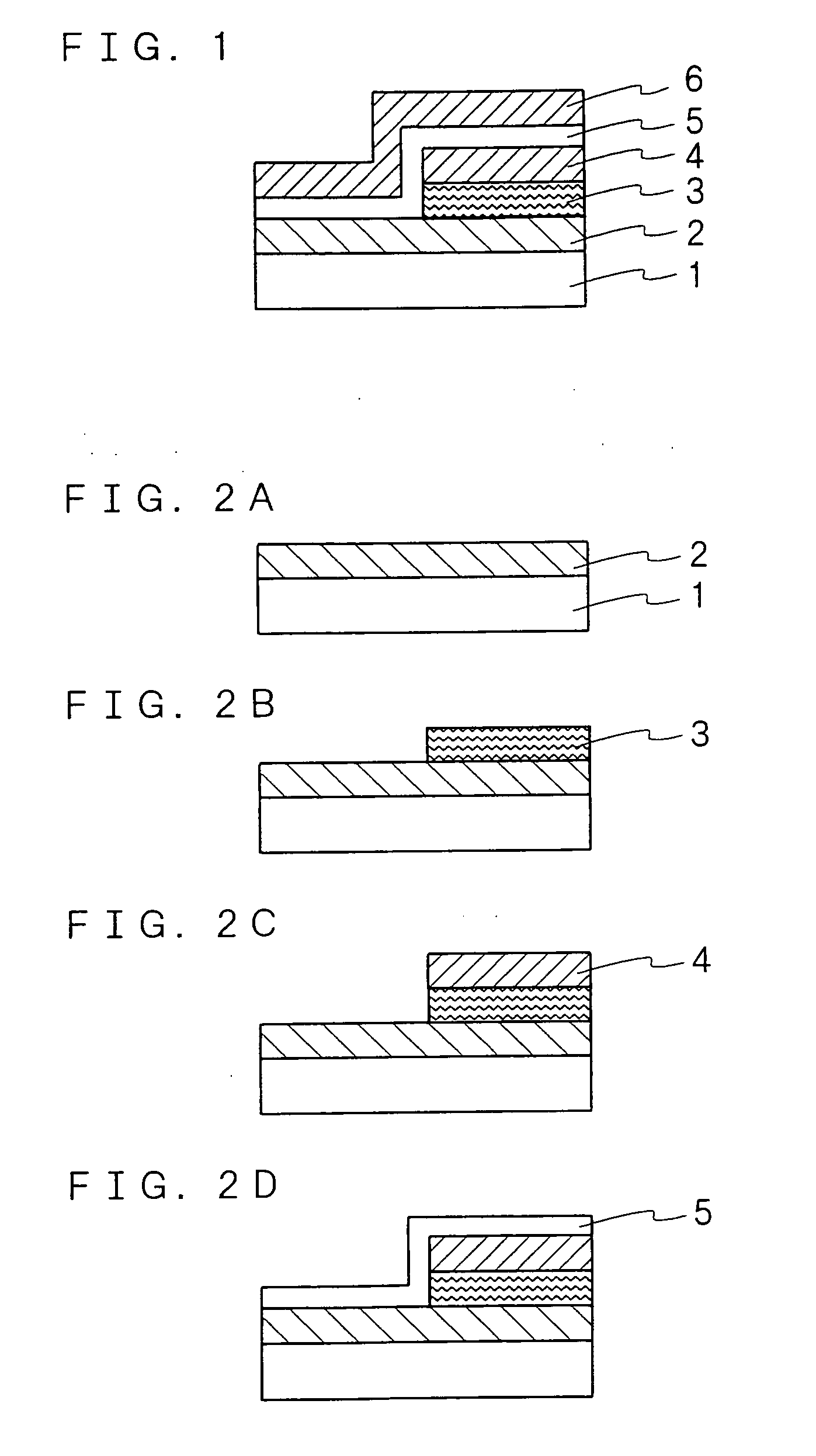
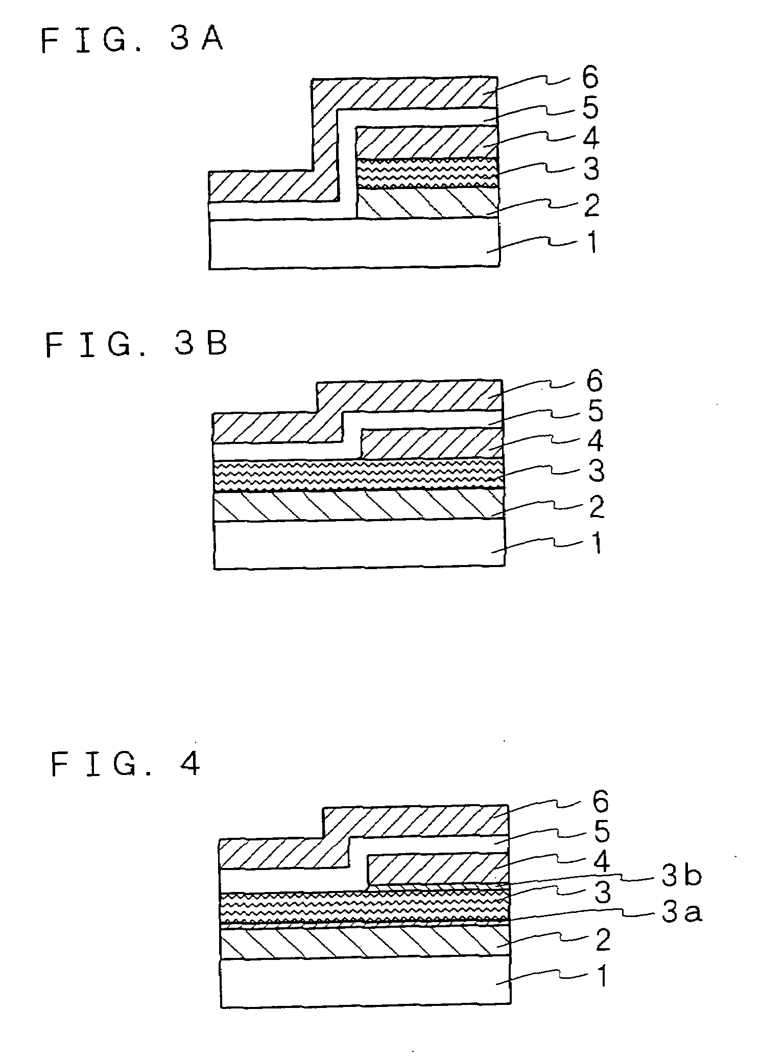
[0046]An organic semiconductor element of the present invention and an organic EL display device using the same are explained below with reference to the drawings. In the organic semiconductor element of the present invention, as shown in the sectional explanatory diagram of one embodiment in FIG. 1, a first conductive layer 2 which is one of source / drain electrodes is provided onto a substrate 1, and an organic semiconductor layer 3 and a second conductive layer 4 which is the other electrode of the source / drain electrodes are provided onto the first conductive layer 2. In the example shown in FIG. 1, the organic semiconductor layer 3 and the second conductive layer 4 are formed so as to be smaller than the first conductive layer 2, and a part of the first conductive layer 2 is exposed. A gate electrode (third conductive layer) 6 is provided to the surface of the first conductive layer 2 via an insulating layer 5 as a gate insulating film so that an FET is formed. The substrate 1 i...


PUM


Abstract

It is provided an organic semiconductor element having an FET which can control a channel length to a small value and does not cause a rise in contact resistance due to a step portion, and an organic light emitting display device with a large aperture using the same. A first conductive layer (2) which is one of source/drain electrodes is provided onto a substrate (1), and an organic semiconductor layer (3) and a second conductive layer (4) which is the other electrode of the source/drain electrodes are provided onto the first conductive layer (2). Then on a side face of the organic semiconductor layer or a front surface of the organic semiconductor layer (3) exposed by removing a part of the second conductive layer and a side face of the second conductive layer a gate electrode (third conductive layer) (6) is provided via an insulating layer (5), thereby to form an FET. The organic EL display device has the FET having such structure laminated on an organic EL section as a drive element.

Description

TECHNICAL FIELD[0001]The present invention relates to an organic semiconductor element including a field-effect transistor (hereinafter, FET) or the like using an organic semiconductor, and an organic EL display device using the same. More specifically, the present invention relates to an organic semiconductor element which can make a channel length very short while using an organic semiconductor and can compose a display device only by laminating an organic EL section, and an organic EL display device using the same.BACKGROUND ART[0002]As structures of conventional FETs using organic semiconductor layers, structures shown in FIGS. 9A to 9C are known. That is, the structure shown in FIG. 9A is called a bottom contact (BC) structure. For example, a pair of source / drain electrodes 33 and 34 are provided onto an insulating film 32 on a gate electrode 31 composed of a silicon substrate, and an organic semiconductor layer 35 is provided thereon, so that the organic semiconductor layer 35...

Claims


Application Information

Patent Timeline
Patent Type & Authority Applications(United States)
IPC IPC(8): H01L51/00H01L27/32H01L29/786H01L51/05
CPCH01L27/3248H01L27/3262H01L27/3265H01L27/3274H01L51/0541H01L51/0545H01L51/057H10K59/123H10K59/1213H10K59/1216H10K59/125H10K10/491H10K10/464H10K10/466
Inventor OKUYAMA, SUGURUSHIMOJI, NORIYUKI
Owner ROHM CO LTD
Why Eureka
Try Eureka