Electroluminescent device having improved contrast

a technology of electroluminescent devices and contrast, which is applied in the direction of semiconductor devices, electrical equipment, material nanotechnology, etc., can solve the problems of high manufacturing cost, low light output efficiency, and difficulty in combining multi-color output from the same chip, so as to increase the ambient contrast of an electroluminescent device and reduce the light emission of the electroluminescent device

Inactive Publication Date: 2008-10-02
EASTMAN KODAK CO
View PDF5 Cites 97 Cited by
  • Summary
  • Abstract
  • Description
  • Claims
  • Application Information

AI Technical Summary

Benefits of technology

[0015]The present invention has the advantage that it increases the ambient contrast of an electro...

Problems solved by technology

The dominant ones are high manufacturing costs; difficulty in combining multi-color output from the same chip; efficiency of light output; and the need for high-cost rigid substrates.
However, in comparison to crystalline-based inorganic LEDs, OLEDs suffer reduced brightness, shorter lifetimes, and require expensive encapsulation for device operation.
Because of problems such as aggregation of the quantum dots in the emitter layer, the efficiency of these devices was rather low in comparison with typical OLED devices.
The efficiency was even poorer when a neat film of quantum dots was used as the emitter layer (Hikmet et al., Journal of Applied Physics 93, 3509 (2003)).
The poor efficiency was attributed to the insulating nature of the quantum-dot layer.
Regardless of improvements in efficiency, these hybrid devices still suffer from all of the drawbacks associated with pure OLED devices.
The resulting device had a poor external quantum efficiency of 0.001 to 0.01%.
These organic ligands are insulators and would result in poor electron and hole injection onto the quantum dots.
In addition, the remainder o...

Method used


Image

  • Electroluminescent device having improved contrast
  • Electroluminescent device having improved contrast
  • Electroluminescent device having improved contrast

Examples


Embodiment Construction

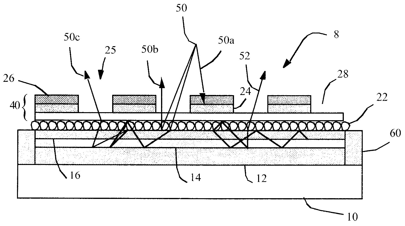
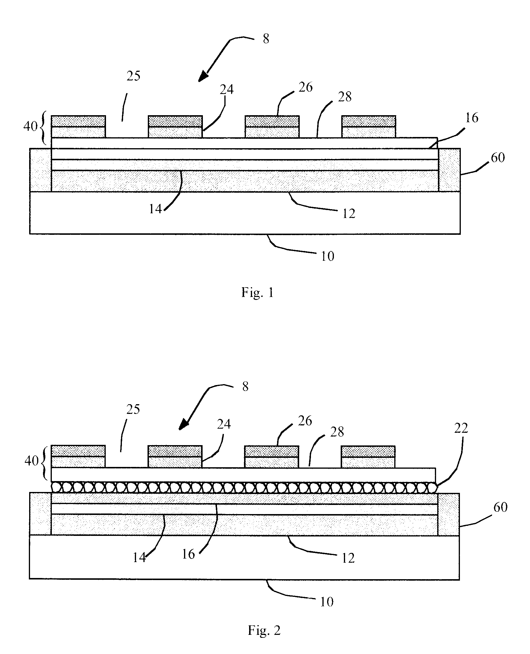
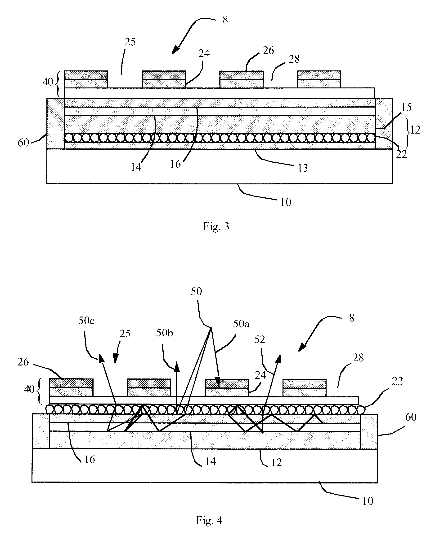
[0034]According to one embodiment of the present invention, an electroluminescent (EL) device comprises a first electrode and a second electrode having an EL unit formed there-between, wherein the second electrode is transparent and a contrast-enhancement element is formed on a side of the second electrode opposite the EL unit and has a geometric area for controlling ambient light contrast ratio of the electroluminescent device. As used herein, a geometric area is a spatial area having a shape and an opening within the spatial area also having a shape. The openings for the contrast enhancement element are transparent in several of the exemplary embodiments disclosed herein. In a typical embodiment, at least one of the electrodes is patterned to form discrete light-emitting areas and the shape of the geometric area corresponds to the shape of the patterned light-emitting area.

[0035]In a further embodiment of the present invention, the contrast enhancement element comprises a transpar...


PUM


Abstract

A method for increasing ambient light contrast ratio within an electroluminescent device, including: a reflective electrode and a transparent electrode having an EL unit formed there-between. The EL unit includes a light-emitting layer containing quantum dots. Additionally, the method includes locating a contrast enhancement element on a side of the transparent electrode opposite the EL unit. The contrast enhancement element includes a patterned reflective layer and a patterned light-absorbing layer whose patterns define one or more transparent openings, so that light emitted by the light-emitting layer passes through the one or more transparent openings. The patterned reflective layer is located between the patterned light absorbing layer and the transparent electrode.

Description

FIELD OF THE INVENTION[0001]The present invention relates to electroluminescent devices having emissive quantum dots; and more particularly, to electroluminescent device structures for improving light output and contrast.BACKGROUND OF THE INVENTION[0002]Semiconductor light emitting diode (LED) devices, which are primarily inorganic, have been made since the early 1960's and currently are manufactured for usage in a wide range of consumer and commercial applications. The layers comprising the LEDs are based on crystalline semiconductor materials. These crystalline-based inorganic LEDs have the advantages of high brightness, long lifetimes, and good environmental stability. The crystalline semiconductor layers that provide these advantages also have a number of disadvantages. The dominant ones are high manufacturing costs; difficulty in combining multi-color output from the same chip; efficiency of light output; and the need for high-cost rigid substrates.[0003]In the mid 1980's, orga...

Claims


Application Information

Patent Timeline
IPC IPC(8): H01L33/00H01L31/12H01L27/15H01L29/26
CPCB82Y20/00B82Y30/00H01L51/5012H01L51/5281H01L51/5284H10K50/86H10K50/11H10K50/865
Inventor COK, RONALD S.ELLINGER, CAROLYN R.
Owner EASTMAN KODAK CO
Why Eureka
Try Eureka