Semiconductor Element Mounting Substrate, Semiconductor Module, And Electric Vehicle

a technology of semiconductor modules and mounting substrates, applied in semiconductor devices, semiconductor/solid-state device details, cooling/ventilation/heating modifications, etc., can solve the problems of increasing the number of assembly steps, deteriorating heat release performance, and reducing heat release capability, etc., to achieve excellent cooling performance, small thermal resistance, and simple structure

Inactive Publication Date: 2008-10-02
HONDA MOTOR CO LTD +1
View PDF3 Cites 31 Cited by
  • Summary
  • Abstract
  • Description
  • Claims
  • Application Information

AI Technical Summary

Benefits of technology

[0052]In the semiconductor element mounting substrate according to the aforementioned Item [1], since the insulating layer is directly joined to the heat releasing device, the thermal resistance is small and excellent cooling performance can be demonstrated. Moreover, it is simple in structure, and therefore the manufacture steps can be simplified.
[0053]According to the semiconductor element mounting substrate of the invention as recited in the aforementioned Item [2], especially excellent cooling performance can be secured.
[0054]According to the semiconductor element mounting substrate of the invention as recited in the aforementioned Item [3], more excellent cooling performance can be secured, and it is excellent in strength.
[0055]According to the semiconductor element mounting substrate of the invention as recited in the aforementioned Item [4], the joining of the cooling fluid inlet and outlet tubes to the substrate can be performed easily.
[0056]According to the semiconductor element mounting substrate of the invention as recited in the aforementioned Item [5], especially excellent cooling performance can be secured.
[0057]According to the semiconductor element mounting substrate of the invention as recited in the aforementioned Item [6], excellent cooling performance can be secured since the adhesiveness of the insulating layer and the heat releasing device is high. Furthermore, since the insulating layer is more hard to crack than a ceramic insulating layer, it is possible to manufacture a larger substrate.

Problems solved by technology

According to the structure shown in FIG. 10, however, depending on the flatness and / or the surface roughness of the surface for attaching the semiconductor module 50 and the heat releasing device 60, large thermal resistance generates at the portion 57 of the heat conducting grease, which may result in deteriorated heat release performance.
If sufficient heat release performance cannot be obtained, the heat releasing surface area of the heat releasing device must be increased to cope with the increasing heat generation amount, which contradicts the miniaturization of semiconductor modules.
Moreover, this increases the number of assembly steps.
In addition, since adhesive is used as the adhesive layer, the heat release capability declines due to the deteriorated thermal conductivity.

Method used


Image

  • Semiconductor Element Mounting Substrate, Semiconductor Module, And Electric Vehicle
  • Semiconductor Element Mounting Substrate, Semiconductor Module, And Electric Vehicle
  • Semiconductor Element Mounting Substrate, Semiconductor Module, And Electric Vehicle

Examples


example

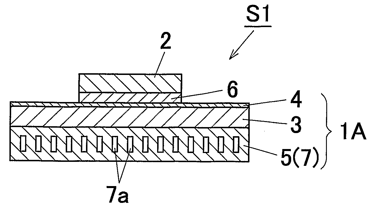
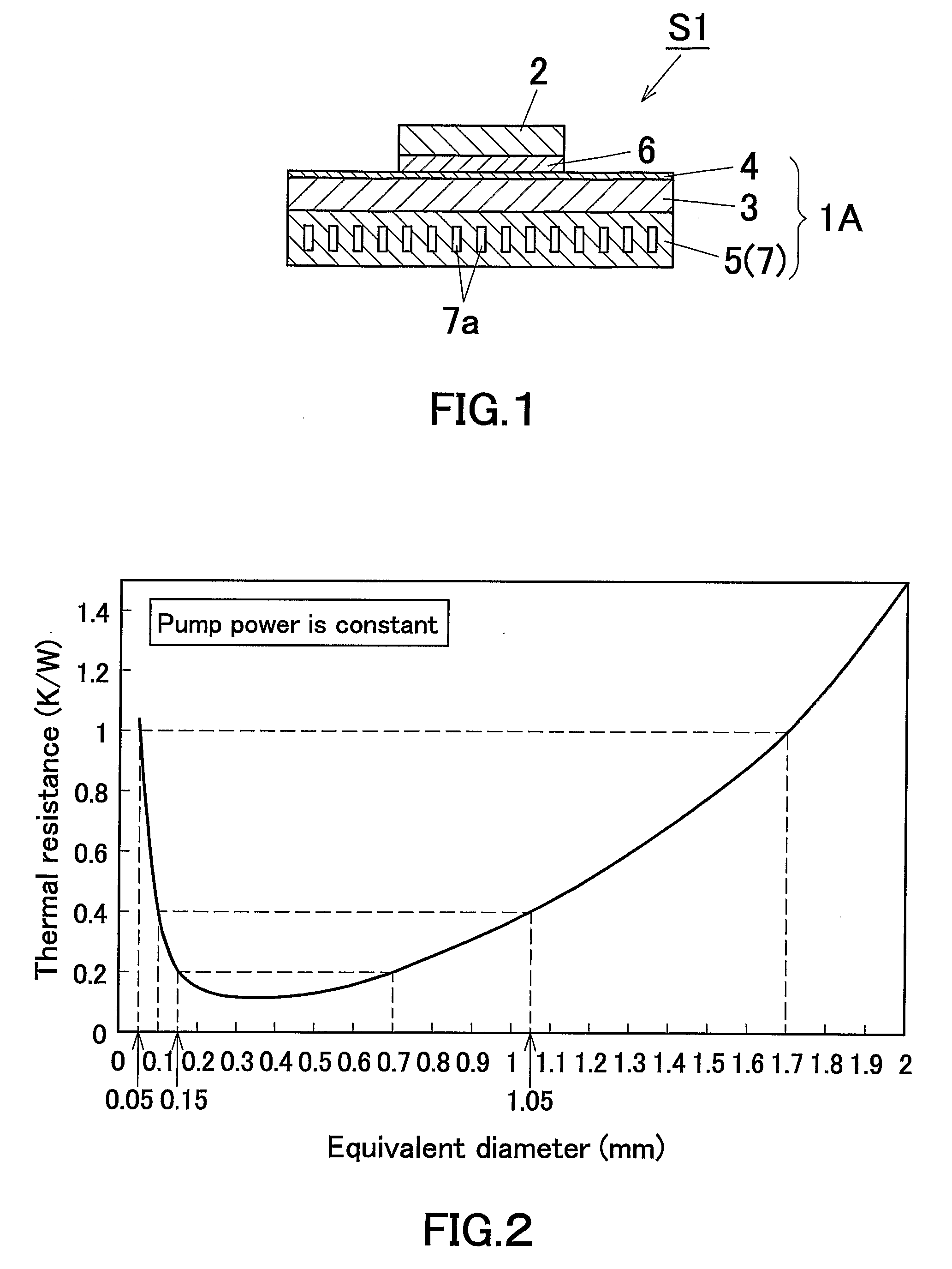
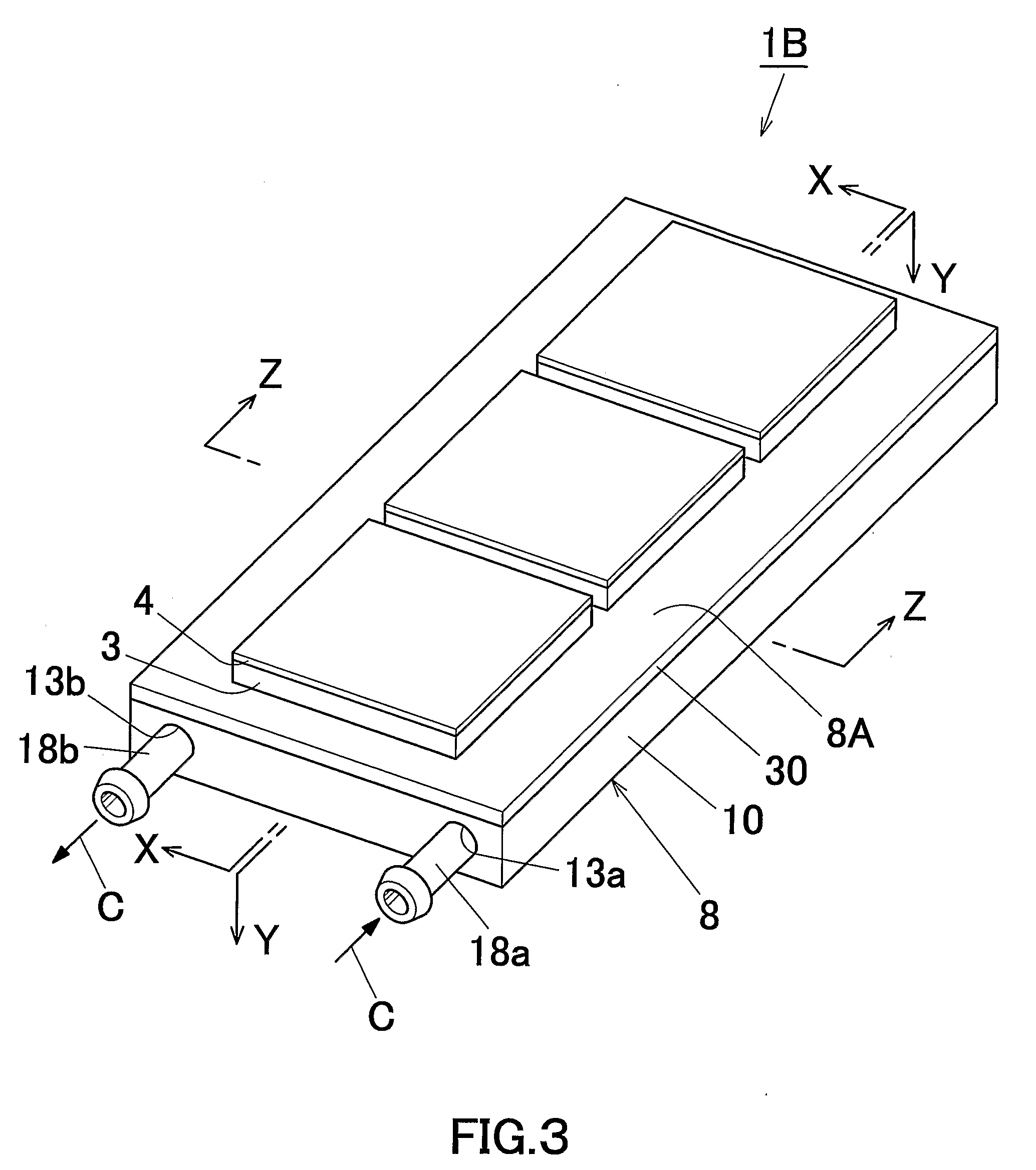
[0121]Semiconductor element mounting substrates 1B and semiconductor modules S2 shown in FIGS. 3 to 7 were manufactured. In the semiconductor element mounting substrates 1B of Examples 1 to 11, the structure of the insulating layer 3 was changed as shown in Table 1 with the conducting layer 4 and the liquid-cooling type cooling plate 8 unchanged.

[0122]As the aforementioned conducting layer 4, a copper foil 70 μm thick was used in each Example.

[0123]As explained above, in the liquid-cooling type cooling plate 8, a plurality of aluminum multi-bored tubes 20 were accommodated in an aluminum case main body 10 and brazed therein, and the first connecting member 18a and the second connecting member 18b were brazed thereto. In detail, each multi-bored tube 20 was an extruded tube with a height of 1.7 mm and a width of 16 mm having 19 fine passages 21. The equivalent diameter of the fine passage 21 was 0.7 mm, the thickness of the peripheral wall was 0.3 mm, and the thickness of the partiti...


PUM


Abstract

A semiconductor element mounting substrate excellent in cooling performance and simple in structure is provided. The semiconductor element mounting substrate is a substrate 1B for mounting a semiconductor element 2, and has an insulating layer 3 and a conducting layer 4 for attaching a semiconductor element 2 on one surface of the insulating layer 3. To the other surface of the insulating layer 3, a heat releasing device 5 is directly attached. The heat releasing device 5 is preferably a liquid-cooling type cooling plate 7 having a plurality of fine passage 7a for cooling fluid. The insulating layer is preferably a composite member that an insulating cloth is impregnated with insulating resin or insulating resin composite in which thermally conductive filler is added to insulating resin.

Description

[0001]This application claims priority under 35 U.S.C. §119 to Japanese Patent Application No. 2004-112205 filed on Apr. 6, 2004, Japanese Patent Application No. 2004-360075 filed on Dec. 13, 2004 and U.S. Provisional Application No. 60 / 561,529 filed on Apr. 13, 2004, the entire disclosures of which are incorporated herein by reference in their entireties.CROSS REFERENCE TO RELATED APPLICATIONS[0002]This application is an application filed under 35 U.S.C. §111(a) claiming the benefit pursuant to 35 U.S.C. §119(e)(1) of the filing date of U.S. Provisional Application No. 60 / 561,529 filed on Apr. 13, 2004, pursuant to 35 U.S.C. §111(b).TECHNICAL FIELD[0003]The present invention relates to a semiconductor element mounting substrate, especially to a semiconductor element mounting substrate having cooling performance.[0004]In this disclosure including claims, the wording of “aluminum” denotes aluminum and its alloy, and the wording of “copper” denotes copper and its alloy.BACKGROUND ART[...

Claims


Application Information

Patent Timeline
Patent Type & Authority Applications(United States)
IPC IPC(8): H05K7/20H01L23/373H01L23/473
CPCH01L23/3735H01L23/473H01L2924/0002H01L2924/00
Inventor AMANO, ATSUSHIURUSHIHARA, KEISUKEKIMURA, KAZUO
Owner HONDA MOTOR CO LTD
Why Eureka
Try Eureka