Method of forming resist pattern and semiconductor device manufactured with the same

a technology of resist pattern and semiconductor device, which is applied in the direction of photomechanical equipment, instruments, originals for photomechanical treatment, etc., can solve the problems of meniscus collapse, film peeling, and the inability to fully expose the liquid, and achieve high water repellent and film peeling suppression

Inactive Publication Date: 2008-10-02
RENESAS ELECTRONICS CORP
View PDF14 Cites 43 Cited by
  • Summary
  • Abstract
  • Description
  • Claims
  • Application Information

AI Technical Summary

Benefits of technology

[0010]An object of the present invention is to provide a method of forming a resist pattern with sufficiently high water-repellency required in liquid immersion exposure and high film-peeling suppression effect, and a semiconductor device manufactured with that method.

Problems solved by technology

If a large amount of the liquid for liquid immersion spills, the meniscus collapses and liquid immersion exposure itself becomes impossible.
In addition, even if an amount of spill is small, the exposure apparatus or a back surface of a substrate is contaminated, which leads to secondary damage causing defocusing due to foreign matters on the back surface of the substrate, in a wafer that is subsequently exposed to light.
Moreover, in liquid immersion exposure of a defective shot, if adhesion of a coating film at a wafer edge to the substrate is weak, the film peels off.
Then, foreign matters that have peeled off from the edge are introduced in the liquid for liquid immersion having flow velocity, the liquid for liquid immersion of wafers is contaminated, and a pattern defect is caused in a center portion of the wafer.
Therefore, water-repellency may be insufficient.
In addition, in order to maintain water-repellency at the wafer outer peripheral portion, removal at edge (hereinafter referred to as edge removal) of a resist or the like around the wafer outer periphery is restricted, and measures against dust production are limited.
Moreover, it is only adhesion between the processed film and a coating film directly on the same that can be improved in order to suppress peeling, and such an improvement is not sufficient as an effect to suppress a pattern defect caused by film peeling.
Foreign matters produced by peeling from a wafer edge float due to convection of the liquid for liquid immersion during liquid immersion exposure and a pattern defect may be induced.
Further, in the conventional water-repellent treatment, water-repellent treatment of the entire surface of the wafer may adversely affect a step of exposure to light, and a method of providing preferred water-repellency to the entire surface has not been studied.

Method used


Image

  • Method of forming resist pattern and semiconductor device manufactured with the same
  • Method of forming resist pattern and semiconductor device manufactured with the same
  • Method of forming resist pattern and semiconductor device manufactured with the same

Examples


example 1

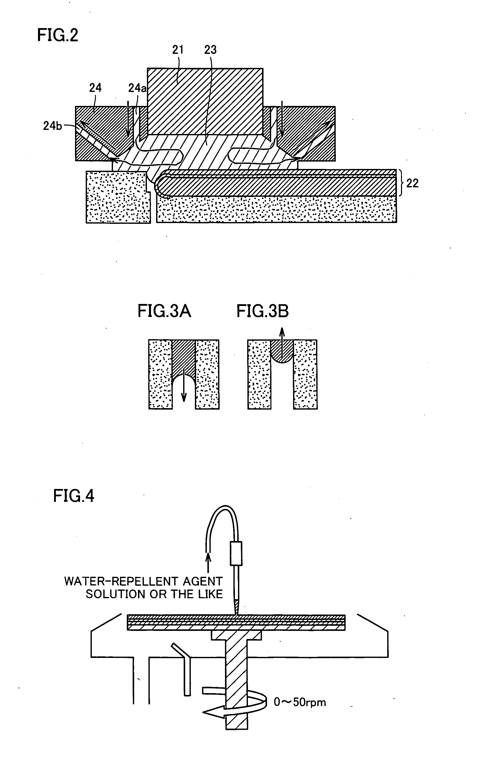
[0065]In order to mainly achieve improvement in water-repellency of an Si wafer, a water-repellent agent solution A including a solvent not dissolving the resist was prepared. In addition, in order to mainly achieve improvement in water-repellency of the Si wafer, a water-repellent agent solution D including the solvent dissolving the resist was prepared. For water-repellent agent solution A, 3,3,3-trifluoropropyltrimethoxysilane (KBM7103 manufactured by Shin-Etsu Chemical Co., Ltd.), tridecafluorohexyltrimethoxysilane (SIT8176-0 manufactured by GELEST Inc.), 2-(3,4-epoxycyclohexyl)ethyltrimethoxysilane (KBM303 manufactured by Shin-Etsu Chemical Co., Ltd.), a mixture of KBM7103 and KBM303 (mixing ratio 3:1), or a mixture of SIT8176-0 and KBM303 (mixing ratio 3:1) was prepared. Each water-repellent agent was dissolved in diisoamyl ether or n-butyl ether, to prepare a dilute solution at a concentration of approximately 3.0 mass %. On the other hand, for water-repellent agent solution ...

example 2

[0070]In the present example, water-repellent agent solution A or a water-repellent agent solution B was employed as the water-repellent agent solution. Water-repellent agent solution A used in Example 1 was also used here. In order to mainly achieve improvement in water-repellency of the organic film, water-repellent agent solution B was prepared by using the solvent not dissolving the resist. As the water-repellent agent, decyltrimethoxysilane (KBM3103C manufactured by Shin-Etsu Chemical Co., Ltd.), KBM7103, or a mixture of KBM3103C and KBM7103 (mixing ratio 1:1) was used. KBM 303 mixed at a mixing ratio of 3:1 with respect to the total mass of the water-repellent agent above was used as the water-repellent agent having adhesion-strengthening effect. Each water-repellent agent was dissolved in diisoamyl ether or n-butyl ether, to prepare a dilute solution at a concentration of 3.0 mass %. In order to avoid hydrolysis of the water-repellent agent, the solvent to be used was dehydra...

example 3

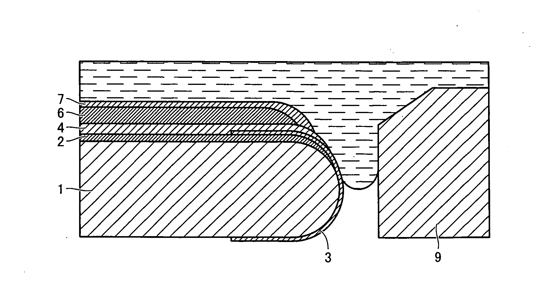
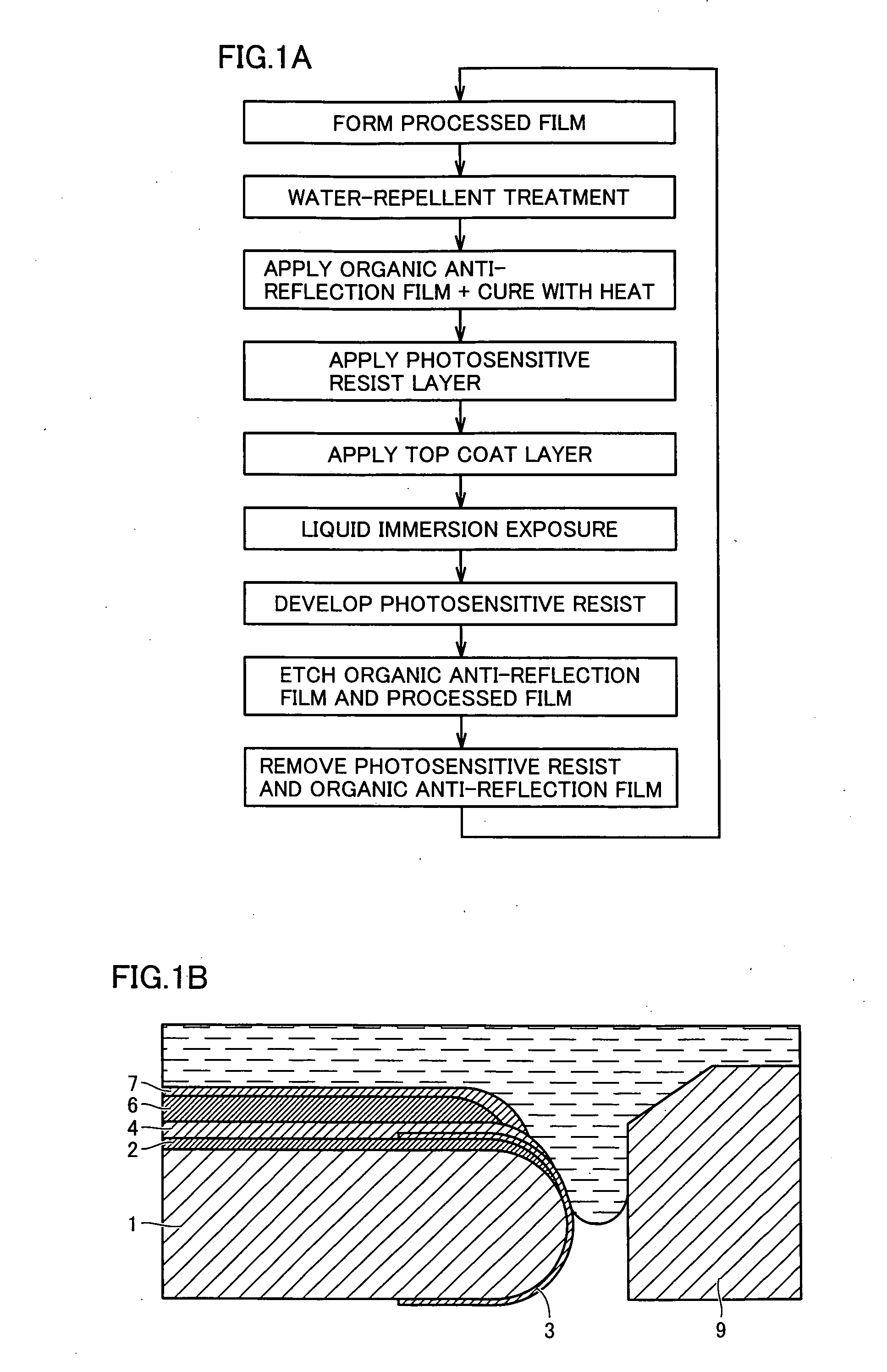
[0073]In the present example, in accordance with the process flow in FIG. 10A, the wafer having the structure shown in FIG. 10B was manufactured. Here, water-repellent agent solution A alone was used as the water-repellent agent solution, water-repellent agent solution B alone was used as the water-repellent agent solution, and a mixture of water-repellent agent solution A and water-repellent agent solution B (mixing ratio 5:5) was used as the water-repellent agent solution. Water-repellent agent solution A used in Example 1 was also used here, and water-repellent agent solution B used in Example 2 was also used here. Initially, after processed film 2 was formed on substrate 1, coating-type organic anti-reflection film 4 was formed to a thickness from approximately 40 nm to 80 nm. The solvent was sufficiently volatilized through heating and curing treatment at 200° C. to 250° C. for approximately 1 to 1.5 minute, and polymers were cross-linked as a result of reaction at a heat react...


PUM

PropertyMeasurementUnit
angle of contactaaaaaaaaaa
widthaaaaaaaaaa

Abstract

A method of forming a resist pattern through liquid immersion exposure in which exposure is performed such that a liquid film is formed between a substrate for a semiconductor device on which a processed film is formed and an objective lens arranged above the substrate is provided, and the substrate treated with a water-repellent agent solution composed of at least a water-repellent agent and a solvent is exposed to light.

Description

BACKGROUND OF THE INVENTION[0001]1. Field of the Invention[0002]The present invention relates to a method of forming a resist pattern with high water-repellency required in liquid immersion exposure and high film-peeling suppression effect, and a semiconductor device manufactured with that method.[0003]2. Description of the Background Art[0004]In forming a resist pattern with liquid immersion type exposure, an apparatus structured as shown in FIG. 2 is used (see Tomoharu Fujiwara et al., “Wafer Management between Coat / Developer Track and Immersion Lithography Tool,” Optical Microlithography XIX edited by Donis G. Flagello, Proc. of SPIE, vol. 6154, 2006). In the liquid immersion type exposure apparatus, a wafer 22 is arranged under a lens 21 and purified water 23 is introduced from an inlet port 24a of a nozzle 24 and ejected from a suction port 24b such that a space between lens 21 and an irradiated surface of wafer 22 is filled with purified water 23. On the irradiated surface, a ...

Claims


Application Information

Patent Timeline
Patent Type & Authority Applications(United States)
IPC IPC(8): H01L23/00B32B3/00G03F7/207
CPCG03F7/11Y10T428/24835G03F7/70341G03F7/2041
Inventor ISHIBASHI, TAKEOTERAI, MAMORUHAGIWARA, TAKUYAYAMAGUCHI, ATSUMI
Owner RENESAS ELECTRONICS CORP
Why Eureka
Try Eureka