

Method for manufacturing semiconductor device
a manufacturing method and semiconductor technology, applied in the direction of semiconductor devices, basic electric elements, electrical appliances, etc., can solve the problems of short communication distance, small antenna size, poor connection, etc., and achieve the effect of preventing partial stretching of semiconductor devices, and preventing damage to semiconductor elements caused by partial stretching
- Summary
- Abstract
- Description
- Claims
- Application Information
AI Technical Summary
Benefits of technology
Problems solved by technology
Method used
Image

Examples
embodiment mode 1
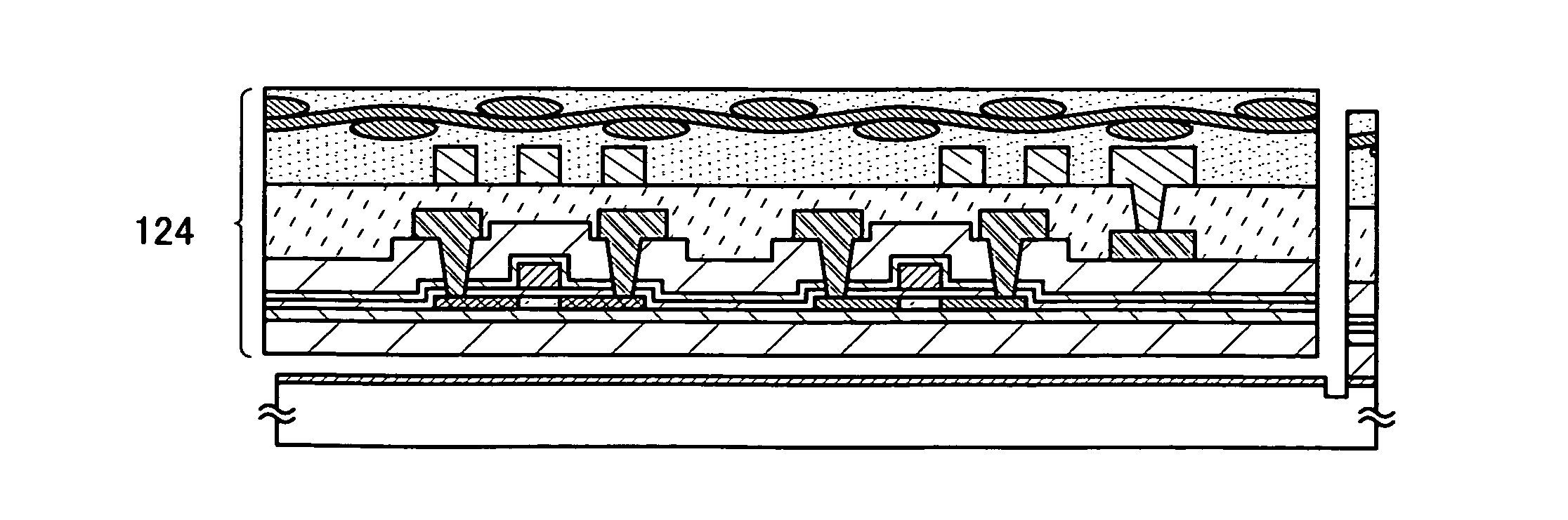
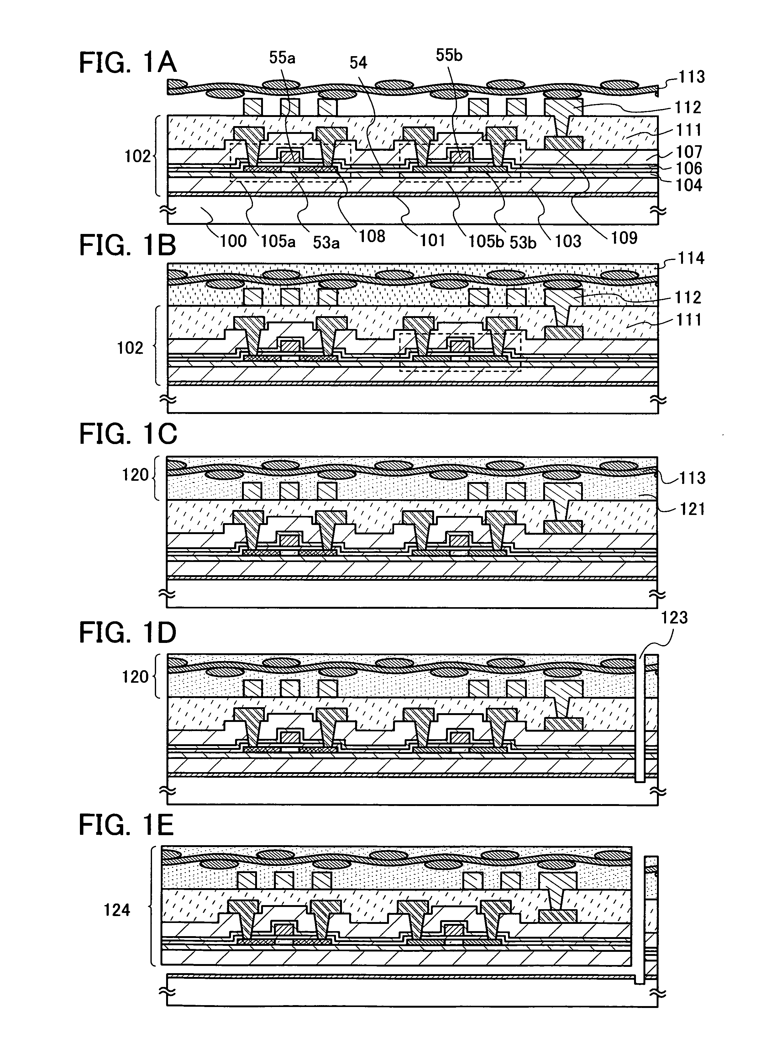
[0037]In this embodiment mode, a method of manufacturing a semiconductor device which is not easily damaged by external local pressure in high yield will be described with reference to FIGS. 1A to 1D.
[0038]As shown in FIG. 1A, a separation layer 101 is formed over a substrate 100 having an insulating surface, and an element layer 102 formed using a semiconductor element formed from a non-single crystal semiconductor layer and an antenna 112 are formed over the separation layer 101. Next, a fibrous body 113 is provided over the element layer 102 and the antenna 112.
[0039]As the substrate 100 having an insulating surface, a substrate which can withstand a temperature at which the element layer 102 and the antenna 112 are formed is preferably used. Typically, a glass substrate, a quartz substrate, a ceramic substrate, a metal substrate in which an insulating layer is formed at least over one surface, an organic resin substrate, or the like can be used. Here, a glass substrate is used a...
embodiment mode 2
[0117]This embodiment mode describes a manufacturing method of a semiconductor device which is not easily destroyed compared with Embodiment Mode 1, with reference to FIGS. 5A to 5D.
[0118]In a similar manner to Embodiment Mode 1, as shown in FIG. 5A, a separation layer 101 is formed over a substrate 100 having an insulating surface, and an element layer 102 including a semiconductor element formed using a non-single crystal semiconductor layer and an antenna 112 are formed over the separation layer 101. Then, a fibrous body 113 is provided over the element layer 102 and the antenna 112, and an organic resin layer 114 is formed, which is followed by the formation of a protective film 131 over the organic resin layer 114.
[0119]The protective film 131 is preferably formed from a high-strength material. As typical examples of a high-strength material, a poly(vinyl alcohol) resin, a polyester resin, a polyamide resin, a polyethylene resin, an aramid resin, a polyparaphenylenebenzobisoxaz...
embodiment mode 3
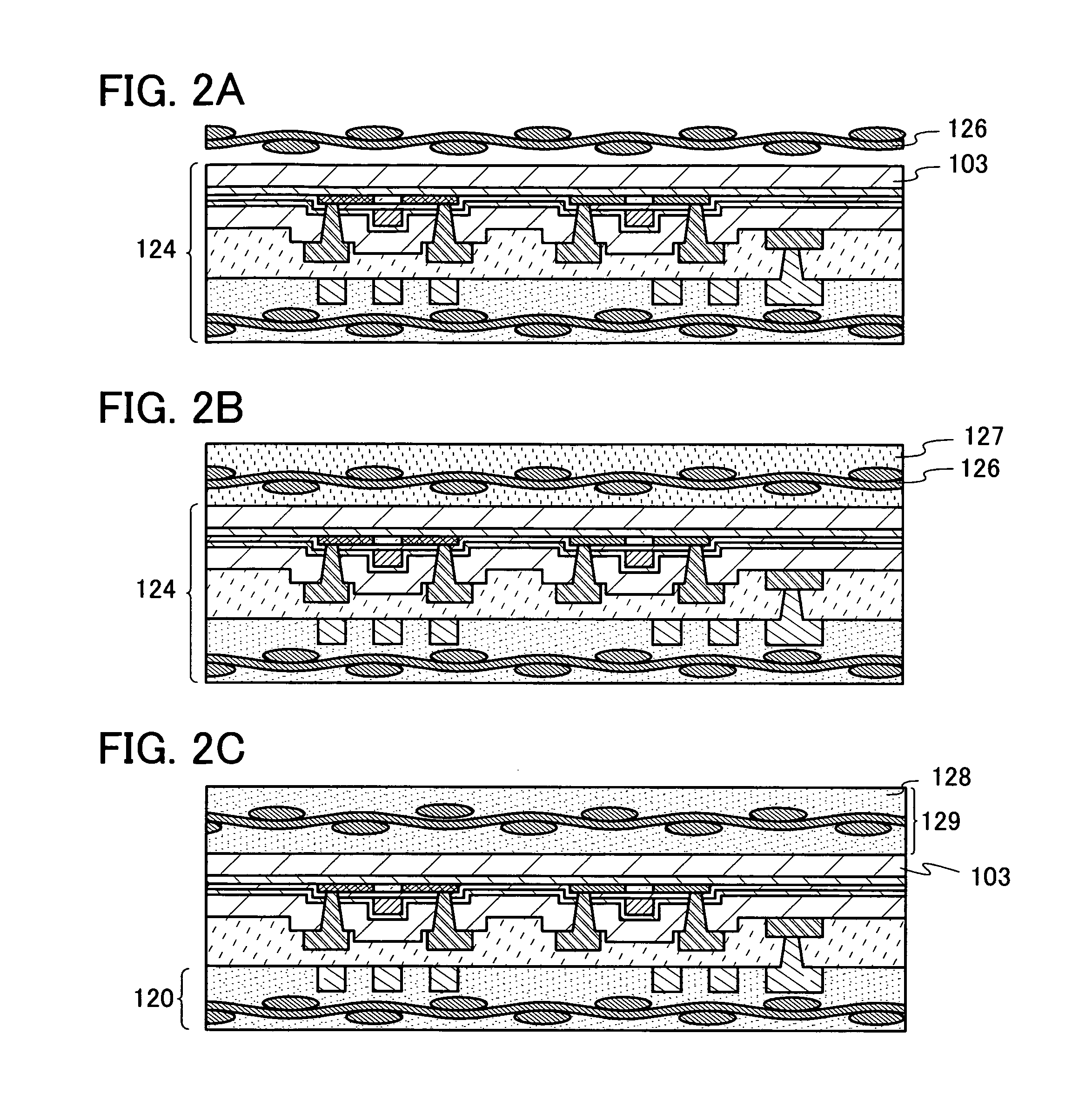
[0129]This embodiment mode describes a method for manufacturing a semiconductor device in which an antenna is not formed in an element layer and an antenna provided over another substrate is connected to the element layer, with reference to FIGS. 6A to 6C and FIGS. 7A to 7C.
[0130]As shown in FIG. 6A, in a similar manner to Embodiment Mode 1, a separation layer 101 is formed over a substrate 100 having an insulating surface, and an element layer 151 including a semiconductor element formed using a non-single crystal semiconductor layer is formed over the separation layer 101. Then, an organic resin layer 155 having the fibrous body and an opening 154 is provided over the element layer 151.
[0131]Here, as the element layer 151, as described in Embodiment Mode 1, an insulating layer 103 serving as a buffer layer is formed, an insulating layer 104 serving as a base layer is formed over the insulating layer 103 serving as a buffer layer, and thin film transistors 105a and 105b are formed ...
PUM
 Abstract
Description
Claims
Application Information