Method of fabricating semiconductor device
- Summary
- Abstract
- Description
- Claims
- Application Information
AI Technical Summary
Problems solved by technology
Method used
Image

Examples
Embodiment Construction
[0017]The following description is of the best-contemplated mode of carrying out the invention. This description is made for the purpose of illustrating the general principles of the invention and should not be taken in a limiting sense. The scope of the invention is best determined by reference to the appended claims.
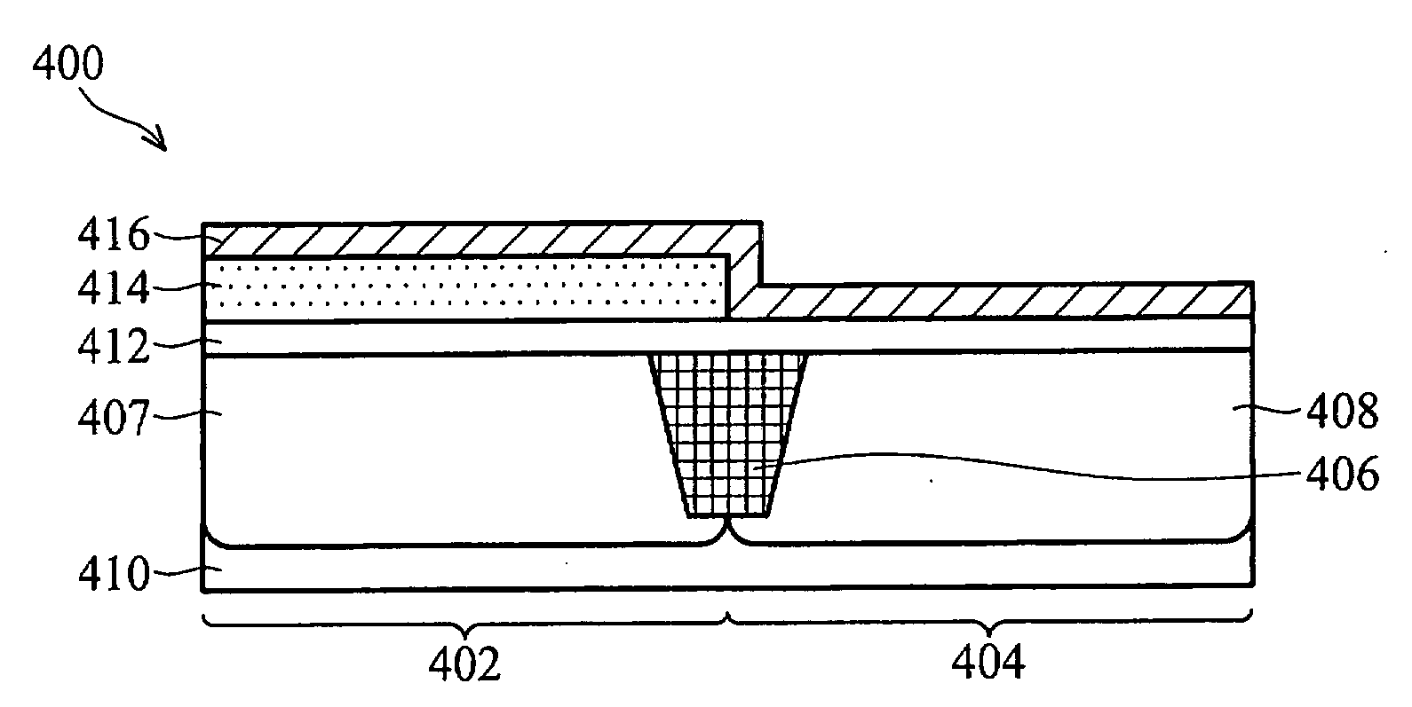
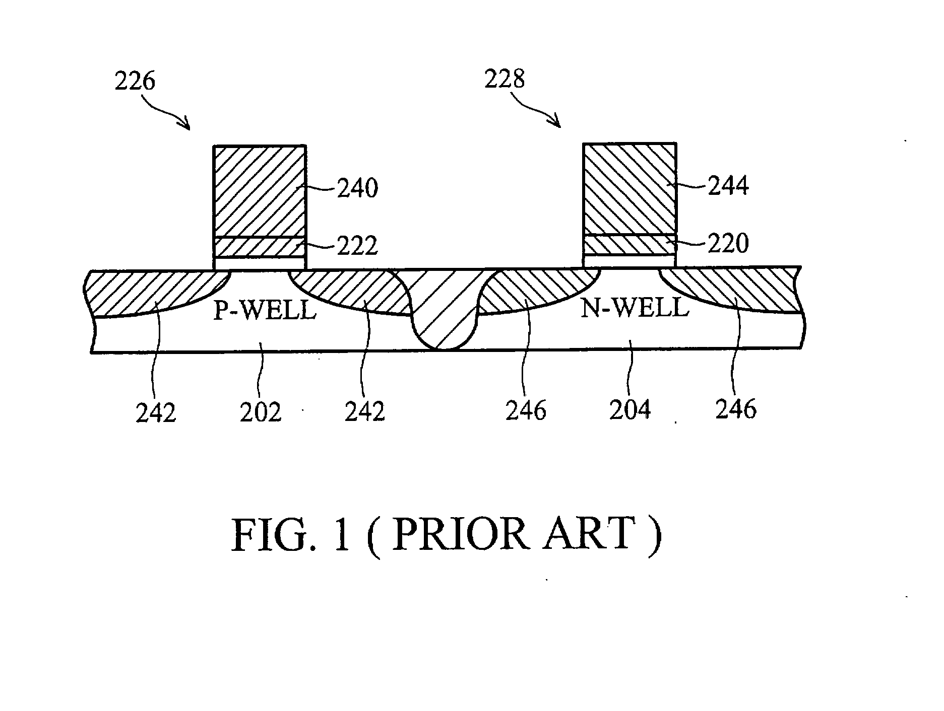
[0018]FIGS. 2a to 2e and FIGS. 3a to 3g show cross sections of various embodiments of a process of fabricating a semiconductor device. Wherever possible, the same reference numbers are used in the drawing and the description to refer the same or like parts.
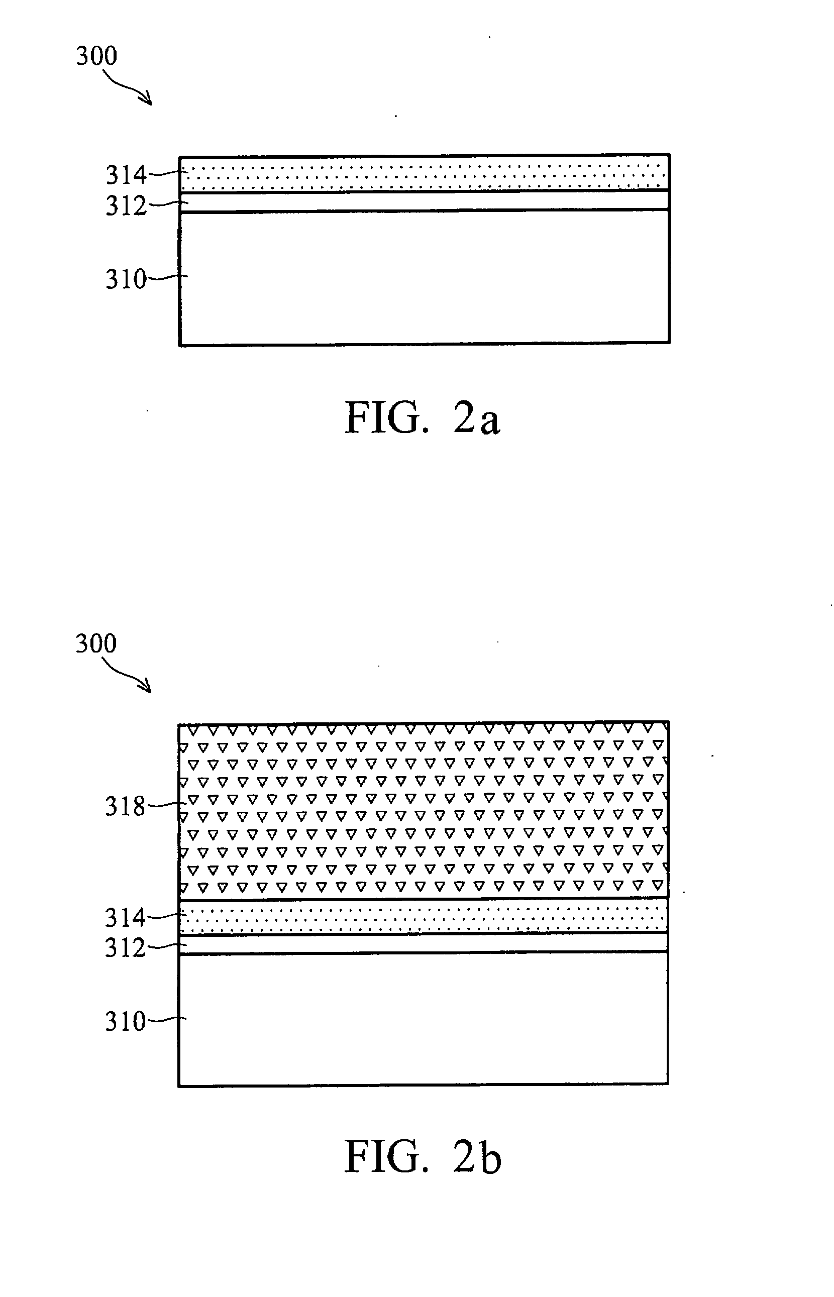
[0019]FIGS. 2a to 2e are cross sections showing an exemplary embodiment of a method for fabricating a MOS device 300. Referring to FIG. 2a, a substrate 310 is provided. The substrate 310 may comprise silicon, SiGe, bulk semiconductor, strained semiconductor, compound semiconductor, silicon on insulator (SOI), and other commonly used semiconductor substrates can be used. The substrate 310 is preferably p-type.
[0020]A ...
PUM
 Abstract
Description
Claims
Application Information
 - R&D Engineer
- R&D Manager
- IP Professional
- Industry Leading Data Capabilities
- Powerful AI technology
- Patent DNA Extraction
Browse by: Latest US Patents, China's latest patents, Technical Efficacy Thesaurus, Application Domain, Technology Topic.
© 2024 PatSnap. All rights reserved.Legal|Privacy policy|Modern Slavery Act Transparency Statement|Sitemap