Migration of integrated circuit layout for alternating phase shift masks

a technology of alternating phase shift mask and integrated circuit, which is applied in the direction of cad circuit design, originals for photomechanical treatment, instruments, etc., can solve the problems of no adequate technique to migrate routing from general topologies to altpsm restricted topologies, and design topology restrictions

Inactive Publication Date: 2008-10-02
IBM CORP
View PDF11 Cites 142 Cited by
  • Summary
  • Abstract
  • Description
  • Claims
  • Application Information

AI Technical Summary

Benefits of technology

[0007]A first aspect of the invention provides a method of migrating an integrated circuit (IC) layout, the method comprising: identifying all jogs in the layout in a first layer including any isolated jogs; identifying clusters of jogs in the first layer that have overlapping jog intervals and extents; first searching for a first open channel portion on the second layer for each of any isolated jogs and in which a respective isolated jog fits without conflict, and in the case that the first open channel portion exists in the second layer, shifting the respective isolated jog to the first open channel portion in the second layer; shifting the cluster of jogs by second searching for a maximal number of second open channel portions on the second layer that intersect each of the jogs intervals, but do not cause the jogs to collide, and first shifting each of the jogs that intersect a second open channel portion to the second layer, and, in the case that the second open channel portion does not exist for at least one remaining jog, determining a new channel on the second layer intersecting an interval of as many of the remaining jogs as possible, and second shifting the remaining jogs of the cluster that have intervals intersecting the new channel to the new channel on the second layer; phase coloring the first layer; and applying a technology migration technique to the first layer and the second layer. One embodiment of the new channel determining includes: a) sorting intervals of the remaining jogs by starting point; b) scanning the IC layout, maintaining a running total of a number of intervals currently active, and maintaining a maximum number of intervals active at any potential new channel position; c) at the maximum number of intervals active at any new channel position, assigning all of t

Problems solved by technology

The use of AltPSM in manufacturing creates topology restrictions in the design.
Unfortunately, no ad

Method used


Image

  • Migration of integrated circuit layout for alternating phase shift masks
  • Migration of integrated circuit layout for alternating phase shift masks
  • Migration of integrated circuit layout for alternating phase shift masks

Examples


Embodiment Construction

I. Introduction and Definitions

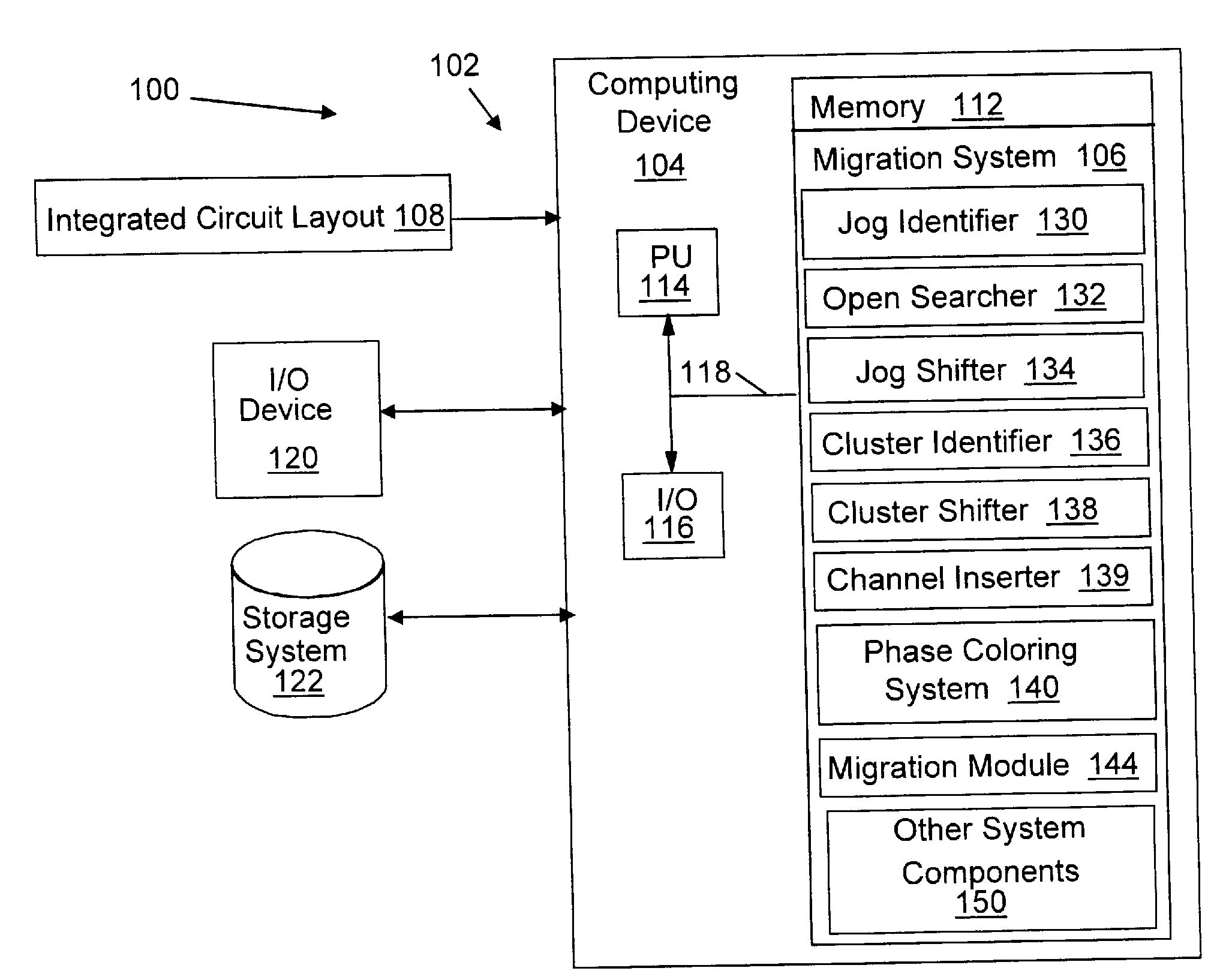
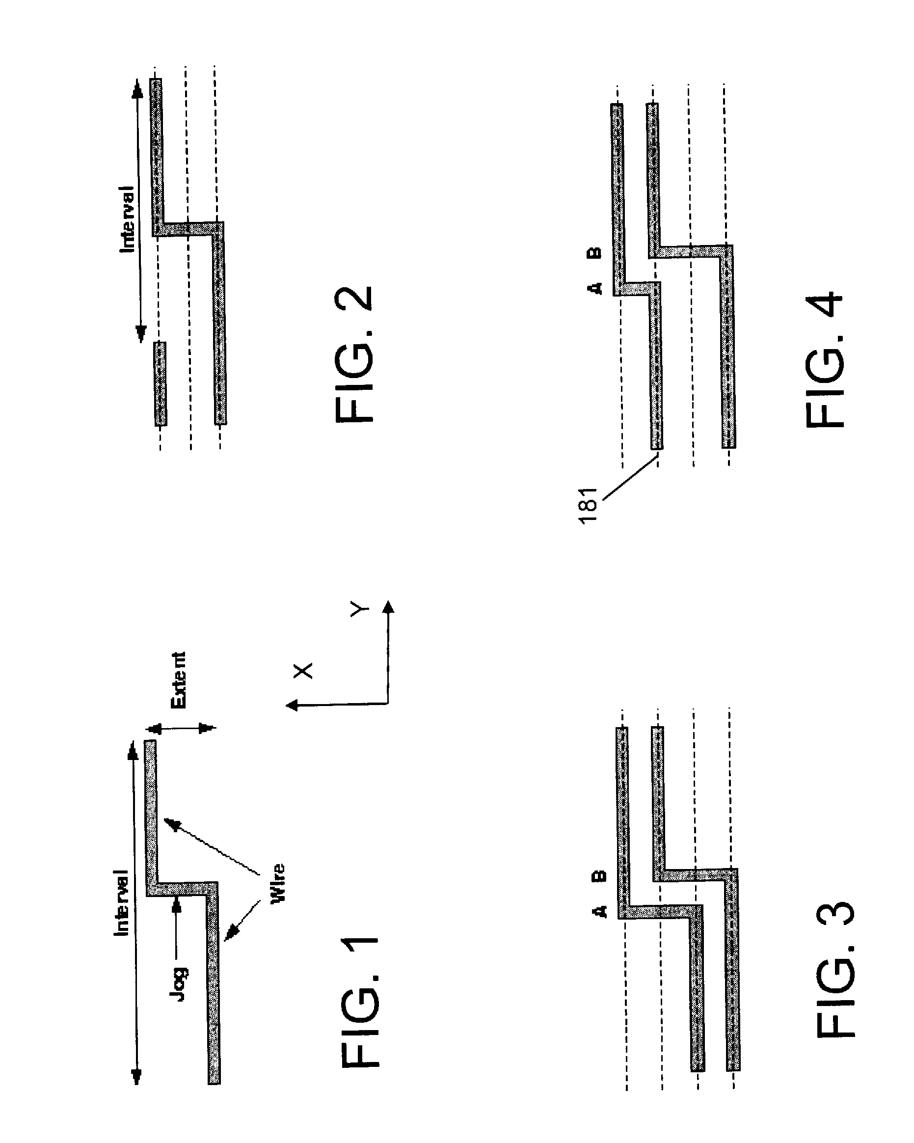
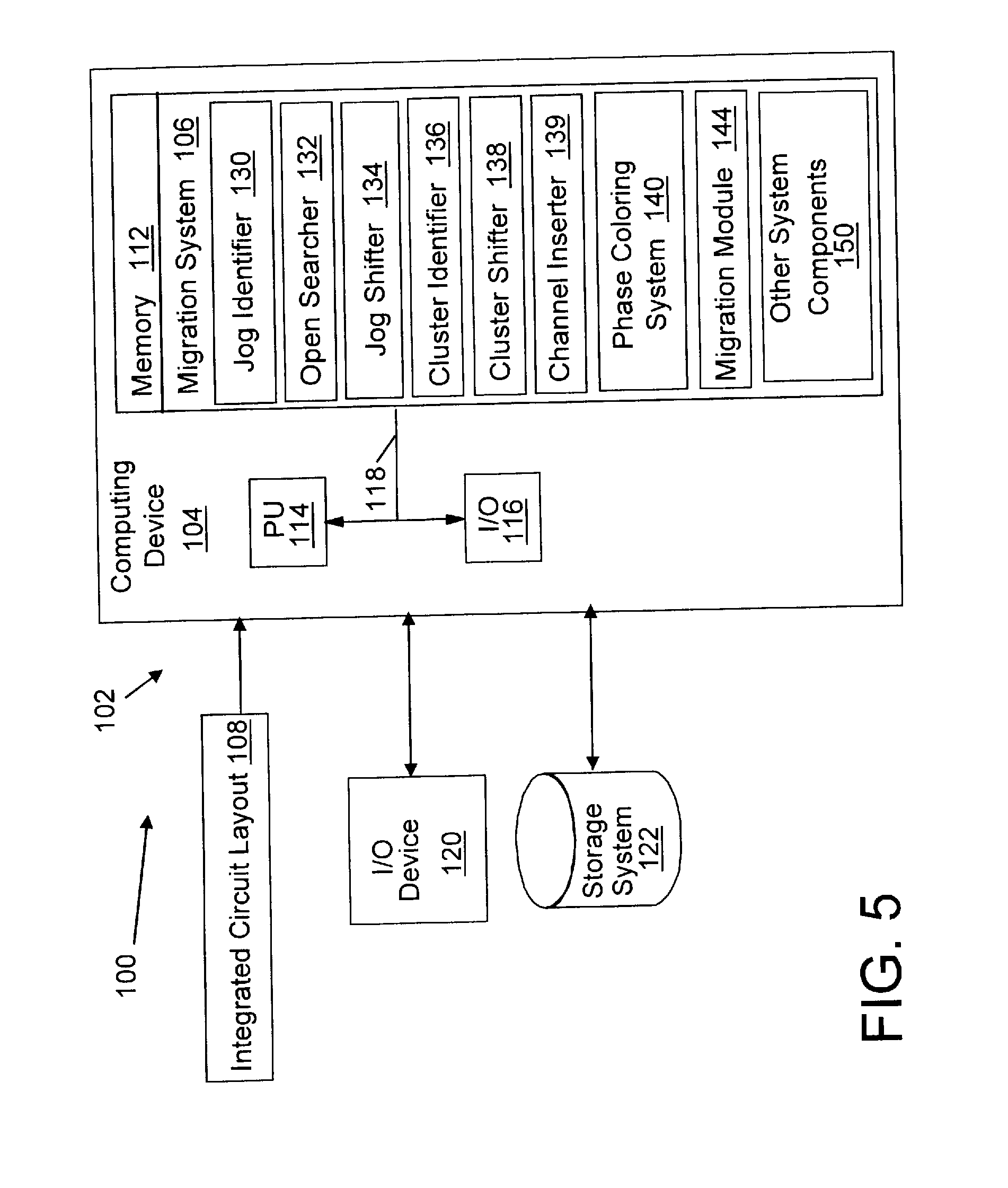
[0023]In order to migrate an integrated circuit (IC) layout from, for example, a non-alternating phase shift masks layout (AltPSM) to an AltPSM layout with phase compliance, jogs on a first, AltPSM layer are identified and shifted to another, second layer. It is understood that while the invention is described relative to AltPSM setting, the teachings of the invention are not so limited. As shown in FIG. 1, a “jog” is a wire that shifts wiring channels, i.e., lines along which wires are laid, within a layer. That is, a segment of wire that does not extend in the preferred wiring direction for the layer in which it exists. Jogs are shifted to the second layer while minimizing the changes to the layout and the number of new wiring channels required. The jog removal process leaves unidirectional wires on the first layer that can be trivially phase colored. Standard technology migration techniques are then used to legalize the results on the layers.

[0024]I...


PUM


Abstract

Method, system and program product for migrating an integrated circuit (IC) layout for, for example, alternating aperture phase shift masks (AltPSM), are disclosed. In order to migrate a layout to phase compliance, jogs are identified on a first (AltPSM) layer and shifted to another second layer. Isolated or clustered jogs are shifted into an open channel portions on the second layer where possible. Remaining clustered jogs are shifted into as few new channels as possible on the second layer. The jog removal process leaves unidirectional wires that can be trivially phase colored. Standard technology migration techniques are then used to legalize the results on the layers.

Description

BACKGROUND OF THE INVENTION[0001]1. Technical Field[0002]The invention relates generally to integrated circuit design, and more particularly, to migrating an integrated circuit (IC) layout for, for example, alternating aperture phase shift masks (AltPSM) or gridded layouts.[0003]2. Background Art[0004]Integrated circuit (IC) chip layouts or designs are created in a graphical computer programming language, and stored in a computer storage medium (such as a disk, tape, physical hard drive, or virtual hard drive such as in a storage access network). If the designer does not fabricate chips or the photolithographic masks used to fabricate chips, the designer transmits the resulting design by physical means (e.g., by providing a copy of the storage medium storing the design) or electronically (e.g., through the Internet) to such entities, directly or indirectly. The stored design is then converted into the appropriate format (e.g., GDSII or Oasis) for the fabrication of photolithographic...

Claims


Application Information

Patent Timeline
IPC IPC(8): G06F17/50
CPCG06F17/5068G03F1/30G06F30/39
Inventor MCCULLEN, KEVIN W.
Owner IBM CORP
Why Eureka
Try Eureka