System, methods and apparatuses for integrated circuits for nanorobotics

Inactive Publication Date: 2008-10-02
SOLOMON RES
View PDF1 Cites 19 Cited by
  • Summary
  • Abstract
  • Description
  • Claims
  • Application Information

AI Technical Summary

Problems solved by technology

Both models present challenges for scientists.
The main challenges to this advanced nanotechnology system lie in the discovery of solutions to the problems of limited information, computation, memory, communicatio

Method used


Image

  • System, methods and apparatuses for integrated circuits for nanorobotics
  • System, methods and apparatuses for integrated circuits for nanorobotics
  • System, methods and apparatuses for integrated circuits for nanorobotics

Examples


Embodiment Construction

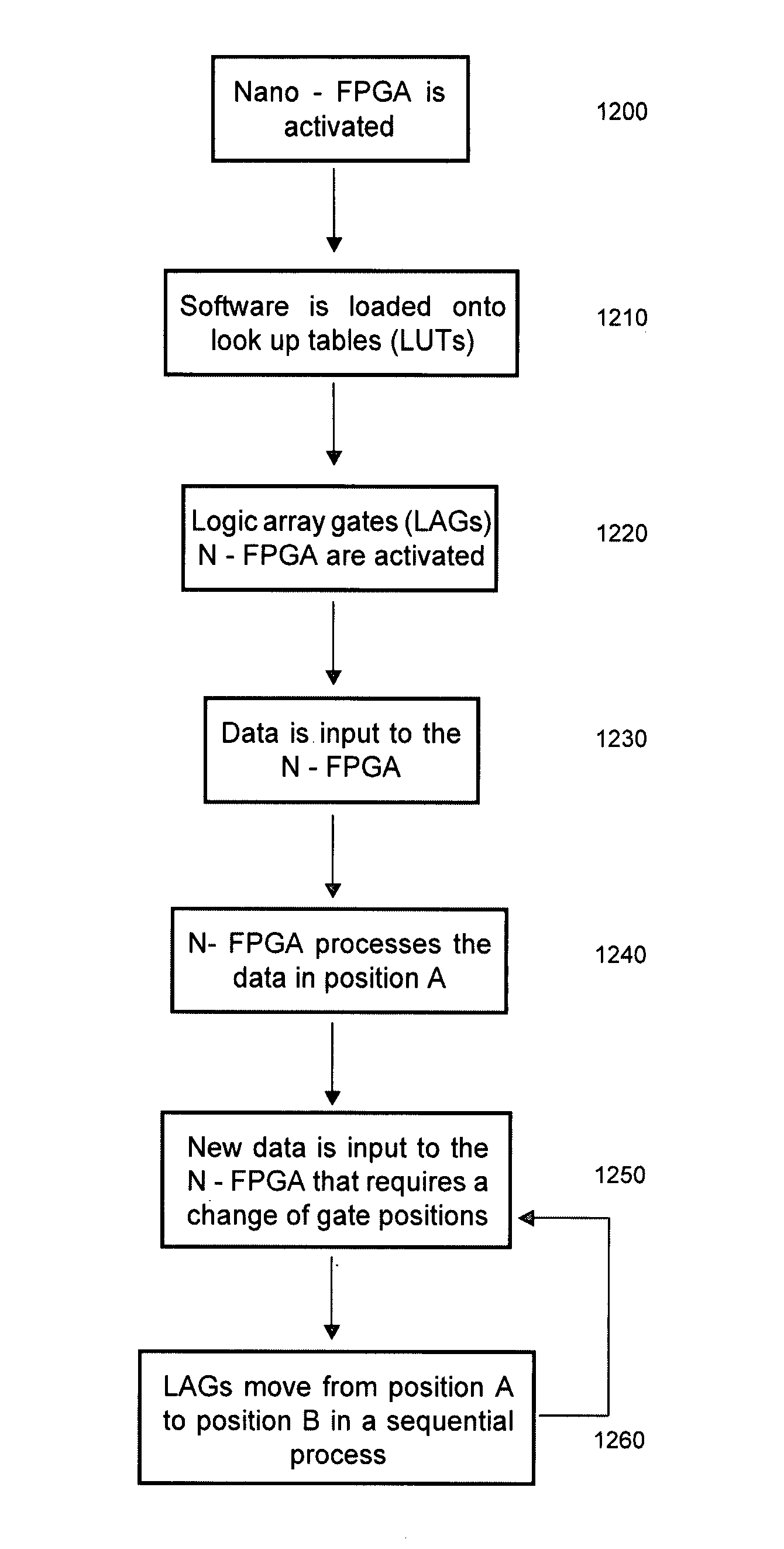
[0054](I) Integrated Circuits in Nano-Robots

[0055]In order to achieve intelligence, it is necessary for nano-scale and micron-scale robotic entities to embody integrated circuits. While trends in ICs have focused on generating the fastest chips with billions of transistors, the current system seeks to develop extremely small, yet highly functional, circuits for use in nanorobots. By interoperating with multiple nanorobots, the intelligent robots are organized into collectives similar to the grid computing paradigm.

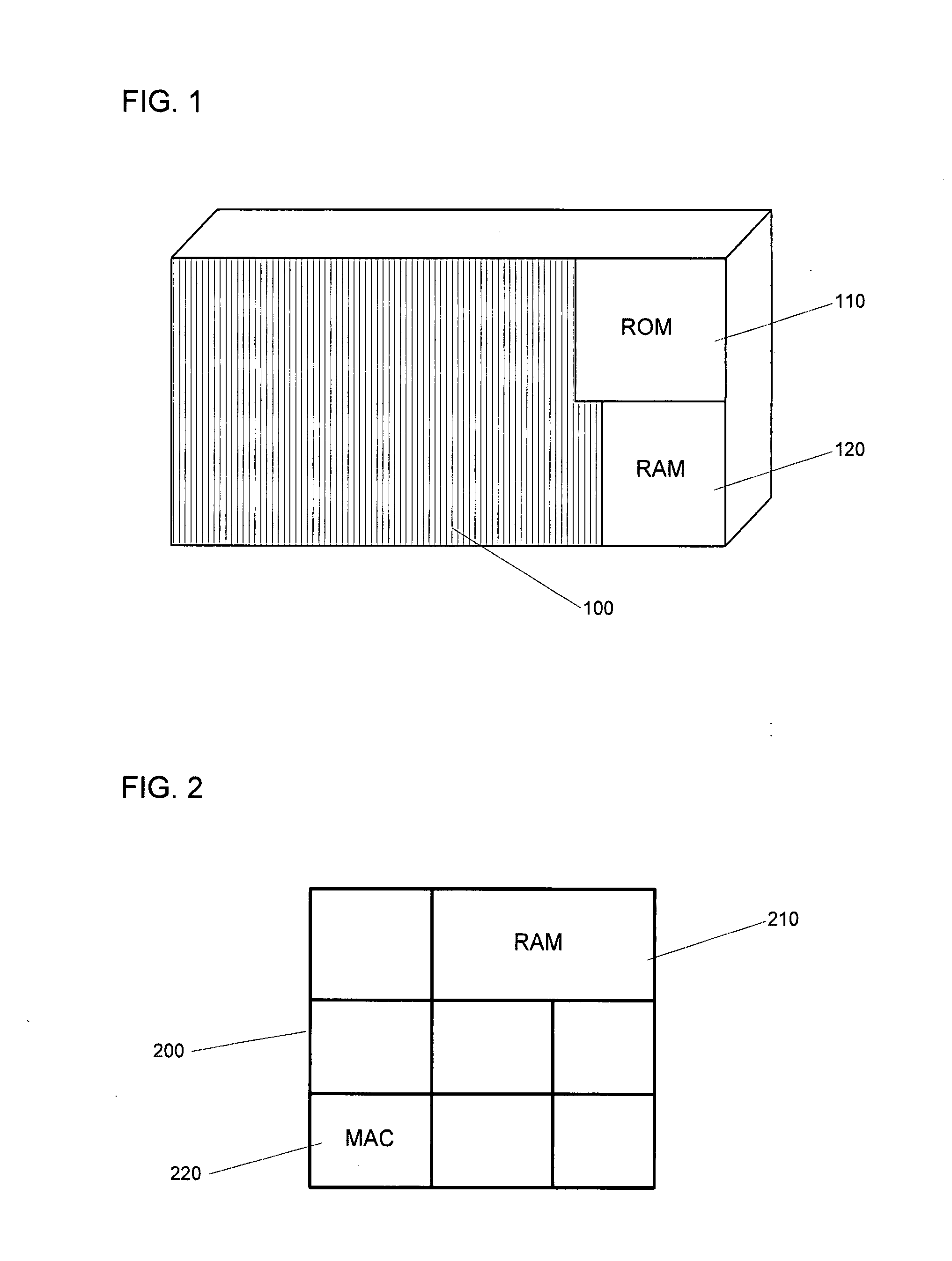
[0056]One main model for nanorobotic ICs is the traditional two dimensional chip approach which employs microprocessor architectures, such as RISC, ASIC and complex programmable logic device (CPLD), such as FPGA architectures. This model integrates logic and memory components using traditional interconnects onto devices in different chip configurations according to each application preference.

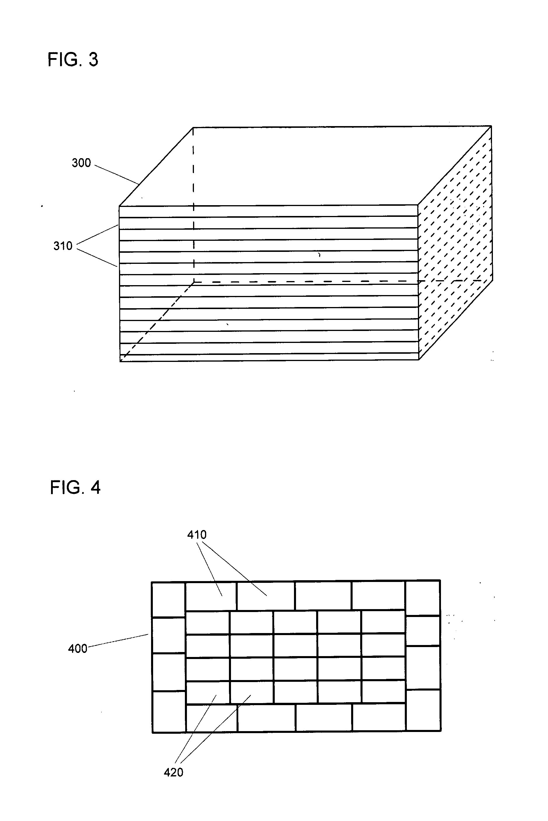
[0057]Another model employs a new generation of efficient three dimensional IC ar...


PUM


Abstract

The invention describes apparatuses for nano-scale integrated circuits applied to nanorobotics. Using EDA techniques, the system develops fully functional nano ICs, including ASICs and microprocessors. Three dimensional nano ICs are disclosed for increased efficiency in nanorobotic apparatuses. Nano-scale FPGAs are disclosed. The nano-scale semiconductors have applications to nano-scale and micro-scale robots.

Description

CROSS-REFERENCES TO RELATED APPLICATIONS[0001]The present application claims the benefit of priority under 35 U.S.C. § 119 from U.S. Provisional Patent Application Ser. No. 60 / 865,605, filed on Nov. 13, 2006 and U.S. Provisional Patent Application Ser. No. 60 / 912,133, filed Apr. 16, 2007, the disclosures of which are hereby incorporated by reference in their entirety for all purposes.FIELD OF THE INVENTION[0002]The present invention pertains to the field of nanotechnology and nanorobotics. The system deals with epigenetic robotics applied to collectives of nanorobots. Specifically, the invention relates to nanoelectromechanical systems (NEMS), microelectromechanical systems (MEMS) and nanomechatronics. The invention also deals with the coordination of collectives of nanorobots and synthetic nanorobots, including synthetic assemblies of NEMS and synthetic nano-scale and micron-scale machine assembly processes. Applications of these systems and processes are made to nanoelectronics, b...

Claims


Application Information

Patent Timeline
IPC IPC(8): G06F17/50
CPCA61B5/0031A61B5/02007A61B5/14532A61B5/411A61B5/416A61B2562/0285B82Y5/00A61B5/41
Inventor SOLOMON, NEAL
Owner SOLOMON RES
Why Eureka
Try Eureka