Embedded metal heat sink for semiconductor

a technology of metal heat sink and optoelectric device, which is applied in the direction of semiconductor lasers, lasers, basic electric elements, etc., can solve the problems of degrading the operational quality of the module, burning out the optoelectrical device, flickering lights, etc., and achieves the effect of increasing the heat-sink efficiency, prolonging the life of the device, and enhancing the stability of the devi

Inactive Publication Date: 2008-10-09
NAT CHENG KUNG UNIV
View PDF5 Cites 3 Cited by
  • Summary
  • Abstract
  • Description
  • Claims
  • Application Information

AI Technical Summary

Benefits of technology

[0012]A semiconductor device is directly embedded into a metal heat sink by directly forming the metal heat sink on the semiconductor device. Then, bonding pads are deposed on the metal heat sink around the semiconductor device for the transition of the electrical connection between the elect

Problems solved by technology

However, when the opto-electrical devices are operated at high power, the temperature of the module composed of the opto-electrical devices increases, thereby degrading the operational quality of the module and ultimately burning out the opto-electrical devices.
However, regarding setting fans in the module, the vibration caused by the operation of the fans results in the lights flickering, and the fans consume additional power.
As a result, the heat generated during the operation of the opto-electrical device mostly accumulates at the connection interfac

Method used


Image

  • Embedded metal heat sink for semiconductor
  • Embedded metal heat sink for semiconductor
  • Embedded metal heat sink for semiconductor

Examples


Embodiment Construction

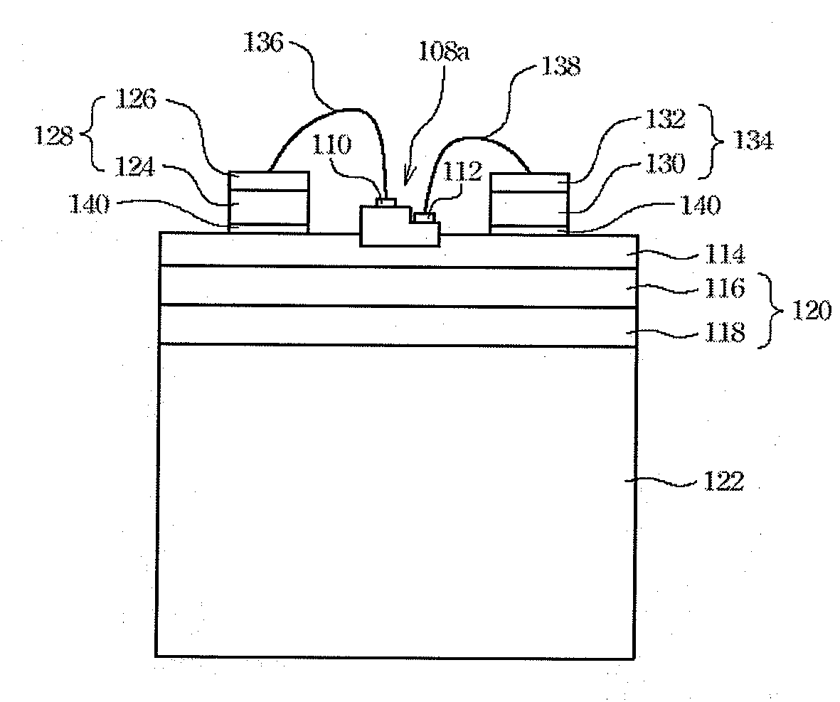
[0015]The present invention discloses an embedded metal heat sink for a semiconductor device and a method for manufacturing the same, in which electrodes of the semiconductor device are in contact with an outer circuit, and the heat-sinking efficiency of the metal heat sink is increased to improve the heat-dissipating problem of the semiconductor device. In order to make the illustration of the present invention more explicit, the following description is stated with reference to FIGS. 1A through 8.

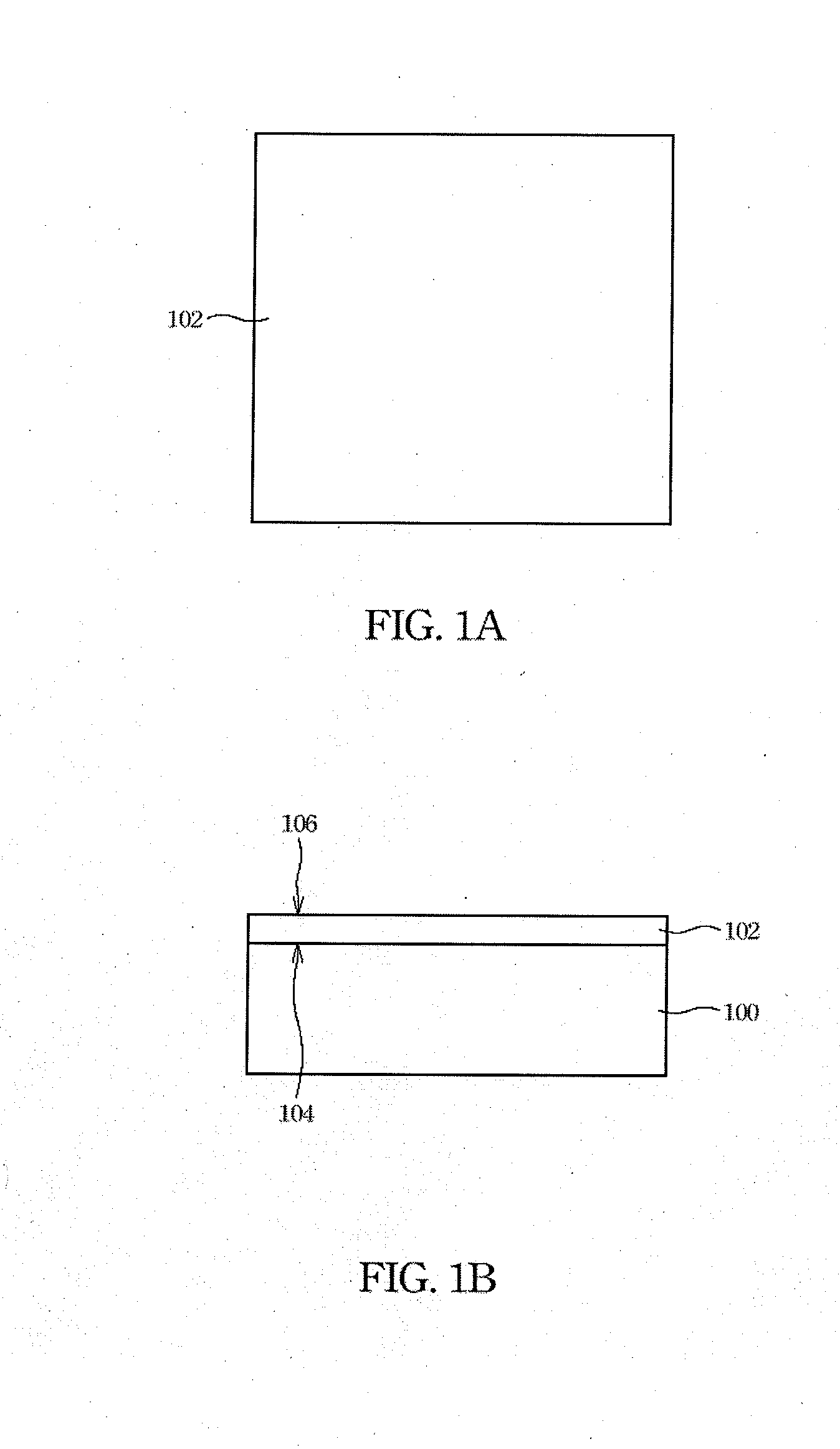
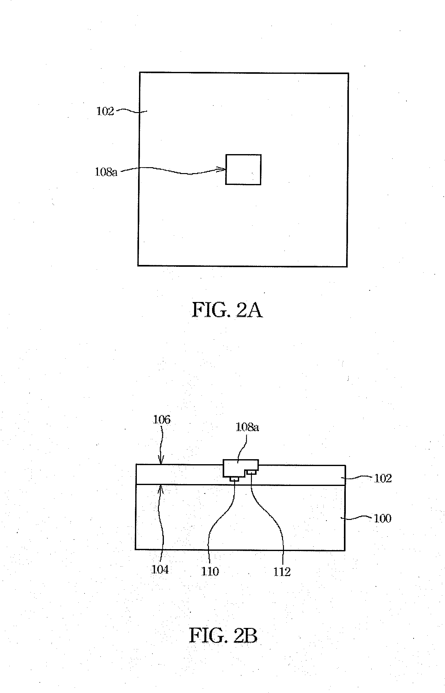
[0016]FIGS. 1A through 8 are schematic flow diagrams showing the process for manufacturing an embedded metal heat sink for a semiconductor device in accordance with a preferred embodiment of the present invention, wherein the schematic flow diagrams includes cross-sectional views and the corresponding top views. In the manufacturing of an embedded metal heat sink of a semiconductor device of the present invention, a temporary substrate 100 and an adhesive tape 102 are initially provided, ...


PUM


Abstract

An embedded metal heat sink for a semiconductor device is described. The embedded metal heat sink for a semiconductor device comprises a metal thin layer, a metal heat sink and two bonding pads. The metal thin layer including a first surface and a second surface on opposite sides, wherein at least one semiconductor device is embedded in the first surface of the metal thin layer, and the semiconductor device has two electrodes with different conductivity types. The metal heat sink is deposited on the second surface of the metal thin layer. The bonding pads are deposed on the first surface of the metal thin layer around the semiconductor device and are respectively corresponding to the electrodes, wherein the electrodes are electrically and respectively connected to the corresponding bonding pads by at least two wires, and the bonding pads are electrically connected to an outer circuit.

Description

RELATED APPLICATIONS [0001]The present application is based on, and claims priority from, Taiwan Application Serial Number 95123020, filed Jun. 26, 2006, the disclosure of which is hereby incorporated by reference herein in its entirety.FIELD OF THE INVENTION [0002]The present invention relates to a metal heat sink and a method for manufacturing the same, and more particularly, to an embedded metal heat sink for an opto-electrical device and a method for manufacturing the same.BACKGROUND OF THE INVENTION [0003]When small solid state opto-electrical devices, such as light-emitting diodes (LEDs) or laser diodes (LDs), are applied in a large or small backlight module or illumination module, many opto-electrical devices are needed to generate sufficient brightness or illumination for the modules. However, when the opto-electrical devices are operated at high power, the temperature of the module composed of the opto-electrical devices increases, thereby degrading the operational quality ...

Claims


Application Information

Patent Timeline
IPC IPC(8): H01L23/36H01L33/62H01L33/64
CPCH01L33/60H01L33/62H01L33/641H01L2224/48091H01L2224/49107H01L2924/01078H01L2924/01079H01S5/0226H01S5/02276H01S5/02469H01L2924/00014H01S5/02345H01S5/0236H01L23/36
Inventor SU, YAN-KUINCHEN, KUAN-CHUNLIN, CHUN-LIANGHUANG, JIN-QUANHU, SHU-KAI
Owner NAT CHENG KUNG UNIV
Why Eureka
Try Eureka