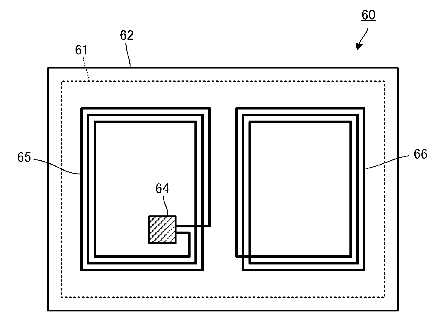
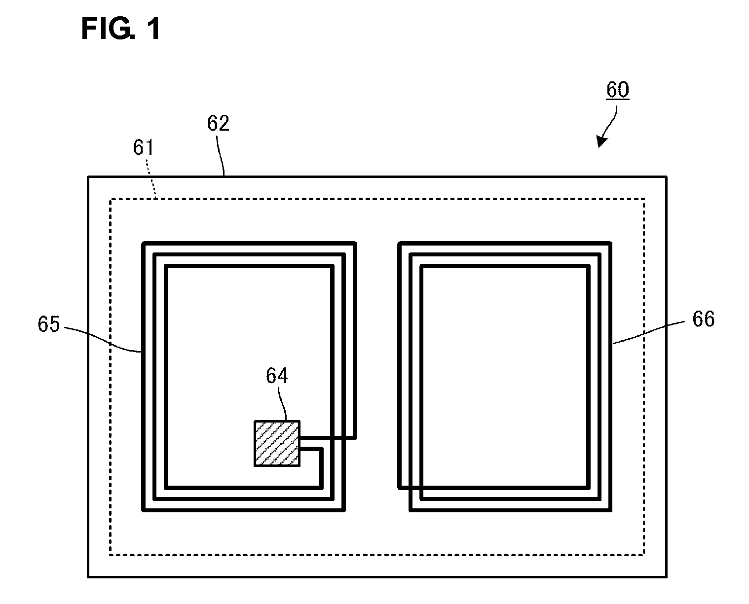
Wireless IC device

a technology of ic device and wire, which is applied in the direction of protective material radiating elements, near-field systems using receivers, instruments, etc., can solve the problems of increasing return loss, disadvantageous size of combination tags described in japanese unexamined patent application publication no. 2007-18067, etc., and achieve excellent radiation characteristics.

Active Publication Date: 2008-10-09
MURATA MFG CO LTD
View PDF18 Cites 38 Cited by
  • Summary
  • Abstract
  • Description
  • Claims
  • Application Information

AI Technical Summary

Benefits of technology

[0008]Preferred embodiments of the present invention provide a small wireless IC device in...

Problems solved by technology

The second antenna 66 consumes energy by resonating in a near electromagnetic field generated by the antenna unit, resulting in an increase in return loss.
However, the size of the combination tag des...

Method used


Image

  • Wireless IC device
  • Wireless IC device
  • Wireless IC device

Examples


first preferred embodiment

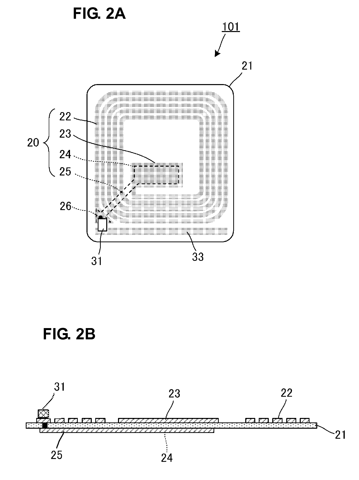
[0031]FIGS. 2A and 2B illustrate the structure of a wireless IC device according to a first preferred embodiment. FIG. 2A is a plan view, and FIG. 2B is a cross-sectional view of a principal portion of the wireless IC device. A wireless IC device 101 includes a substrate (insulating sheet) 21 and a wireless IC 31 including a wireless IC chip mounted on the substrate 21. Various electrodes are also disposed on the substrate 21.

[0032]In FIGS. 2A and 2B, a desired electrode pattern including a conductor such as copper and aluminum is formed on the substrate 21 composed of a resin film such as polyethylene terephthalate (PET) and polypropylene (PP) in the wireless IC device 101. More specifically, a copper foil or an aluminum foil is patterned by etching using a resin sheet on which the copper foil or the aluminum foil is applied.

[0033]As shown in FIGS. 2A and 2B, a substantially spiral line electrode portion 22 and a first capacitance electrode portion 23 connected to the inner end of ...

second preferred embodiment

[0042]FIGS. 4A to 4C are plan views of wireless IC devices according to a second preferred embodiment. The wireless IC device shown in FIGS. 2A and 2B has the linear radiating electrode 33 disposed along a side of the substantially spiral line electrode portion 22 and along a side of the substrate 21. The wireless IC devices shown in FIGS. 4A to 4C have radiating electrodes whose shapes are different from that shown in FIGS. 2A and 2B. In FIG. 4A, a radiating electrode 33a extends along a side of a line electrode portion 22 and along a side of a substrate 21 so as to be turned back.

[0043]In FIG. 4B, a radiating electrode 33b linearly extends along a side of the substrate 21 in a direction away from a radiating / resonating electrode 20.

[0044]In FIG. 4C, a radiating electrode 33c extends along two sides of the substrate 21 so as to have a substantially L-shaped configuration.

[0045]In FIGS. 4A to 4C, structures and operations other than those described above are the same as those in the...

third preferred embodiment

[0048]FIGS. 5A and 5B illustrate the structure of a wireless IC device according to a third preferred embodiment. FIG. 5A is a plan view, and FIG. 5B is a cross-sectional view of a principal part of the wireless IC device. In the wireless IC device shown in FIGS. 2A and 2B, electrodes are disposed on the top and bottom surfaces of the substrate 21 such that capacitance is formed at the capacitance electrode portions that oppose each other with the substrate 21 therebetween. In the wireless IC device shown in FIGS. 5A and 5B, a circuit is formed by utilizing only the top surface of a substrate 21. That is, a substantially spiral line electrode portion 22 and a first capacitance electrode portion 23 connected to the inner end of the line electrode portion 22 are disposed on the top surface of the substrate 21, and an insulating layer 27 is disposed on the electrodes. A second capacitance electrode portion 24 is disposed on the top surface of the insulating layer 27 at a position oppos...


PUM


Abstract

A wireless IC device includes a spiral line electrode portion and a first capacitance electrode connected to the inner end of the line electrode portion, which are disposed on the top surface of a substrate. A second capacitance electrode opposing the first capacitance electrode and a cross line electrode, which connects the second capacitance electrode and a connecting portion that connects the top and bottom surfaces, are disposed on the bottom surface of the substrate. The connecting portion electrically connects the outer end of the line electrode portion and an end of the cross line electrode. A wireless IC is mounted such that terminal electrodes thereof are connected to the connecting portion and an end of a radiating electrode. A radiating/resonating electrode including the line electrode portion, the capacitance electrodes, and the cross line electrode can act both as a resonant circuit for a resonant tag and as a radiating electrode serving as an RFID tag.

Description

BACKGROUND OF THE INVENTION[0001]1. Field of the Invention[0002]The present invention relates to wireless IC devices, and in particular, relates to wireless IC devices using Radio Frequency Identification (RFID) systems enabling data communication using electromagnetic waves in a non-contact manner.[0003]2. Description of the Related Art[0004]Recently, RFID systems enabling information transmission between readers / writers that generate induction fields and RFID tags that store predetermined information on articles in a non-contact manner have been used as systems for controlling articles. Moreover, Japanese Unexamined Patent Application Publication No. 2007-18067 discloses a combination tag including both an RFID tag and a resonant tag.[0005]FIG. 1 illustrates the structure of the combination tag described in Japanese Unexamined Patent Application Publication No. 2007-18067. As shown in FIG. 1, an RFID tag 60 includes an inlet sheet 61 and an overlay sheet 62 that protects surfaces ...

Claims


Application Information

Patent Timeline
IPC IPC(8): H01Q9/04H01Q1/36G06K7/08G06K7/10G06K19/00G06K19/07G06K19/077H01Q1/38H01Q1/40H01Q1/50H01Q5/00H01Q5/10H01Q5/321H01Q5/342H01Q7/00H01Q9/27H01Q21/30H04B5/02
CPCG06K19/07749G06K19/07767H01Q1/2225H01Q1/36
Inventor IKEMOTO, NOBUOKATO, NOBORU
Owner MURATA MFG CO LTD
Why Eureka
Try Eureka