Method of OPC Model Building, Information-Processing Apparatus, and Method of Determining Process Conditions of Semiconductor Device

a semiconductor device and model building technology, applied in the direction of photomechanical equipment, instruments, originals for photomechanical treatment, etc., can solve the problems of difficult to acquire data for measuring, difficult to rule out human-induced sensory differences, and limited length measurement performed in order to build models

Inactive Publication Date: 2008-10-09
HITACHI HIGH-TECH CORP
View PDF7 Cites 12 Cited by
  • Summary
  • Abstract
  • Description
  • Claims
  • Application Information

AI Technical Summary

Benefits of technology

[0007]However, length measurement performed in order to build models is generally limited to a horizontal direction or a vertical direction with respect to a pattern. Consequently, it is currently difficult to acquire data f

Problems solved by technology

However, length measurement performed in order to build models is generally limited to a horizontal direction or a vertical direction with respect to a pattern.
Consequently, it is currently difficult to acquire data for measuring and comparing effects of OPC applied to rectangular corners requiring consideration of oblique components or applied to line ends difficult to compare by simple horizontal and vertical length-measurement values.
Accordingly, it can be said that it is not always possible to rule out human-induced sensory differences (intervention by subjective factors), the uncertainty of judgment criteria, and the like.
In addition, such a conventional method as described above

Method used


Image

  • Method of OPC Model Building, Information-Processing Apparatus, and Method of Determining Process Conditions of Semiconductor Device
  • Method of OPC Model Building, Information-Processing Apparatus, and Method of Determining Process Conditions of Semiconductor Device
  • Method of OPC Model Building, Information-Processing Apparatus, and Method of Determining Process Conditions of Semiconductor Device

Examples


Embodiment Construction

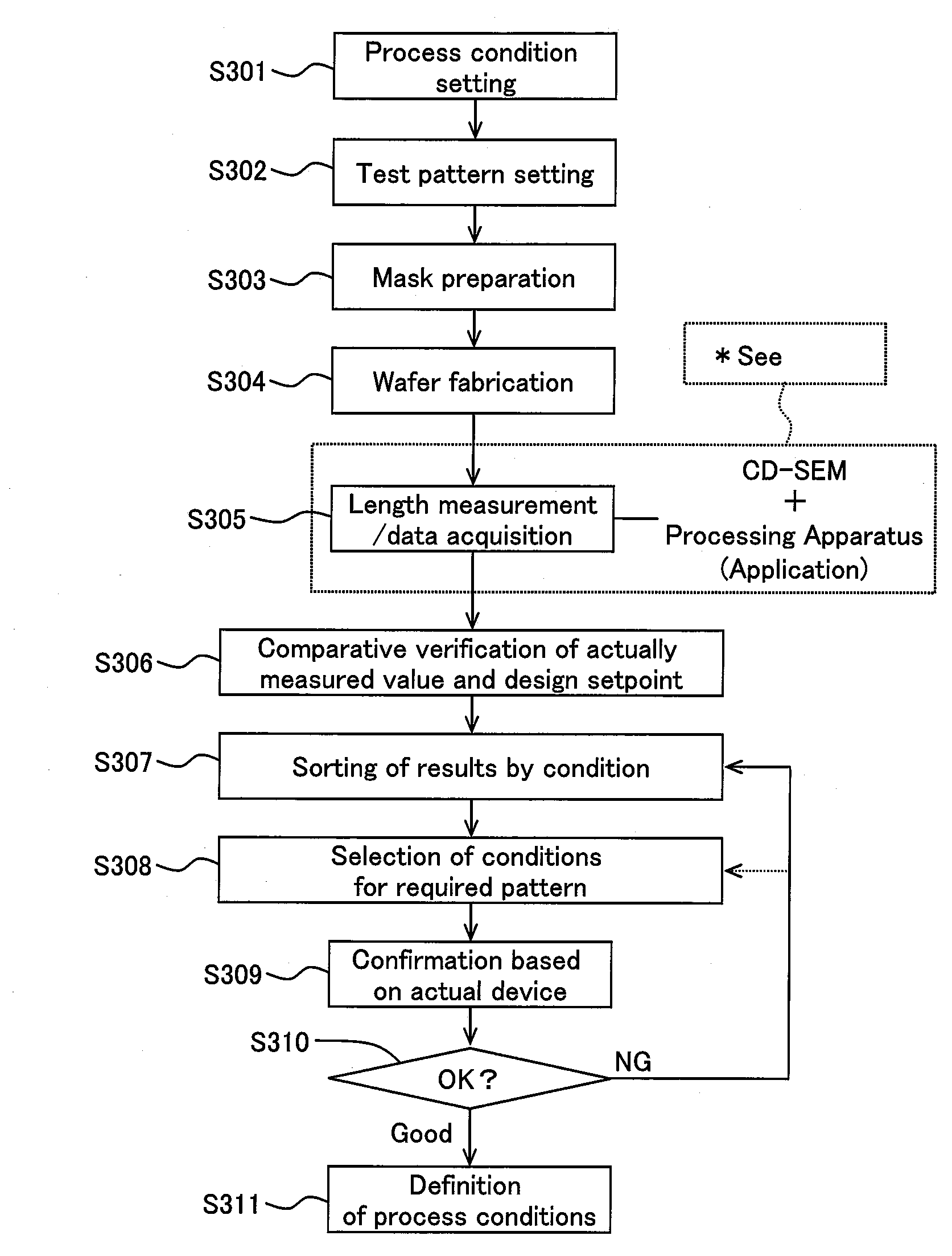
[0032]Now, embodiments of the present invention will be described with reference to the accompanying drawings. It should be noted however that the embodiments described hereinafter are only examples for embodying the present invention and do not limit the invention. In addition, throughout the drawings, like components are denoted by like reference numerals.

[0033]

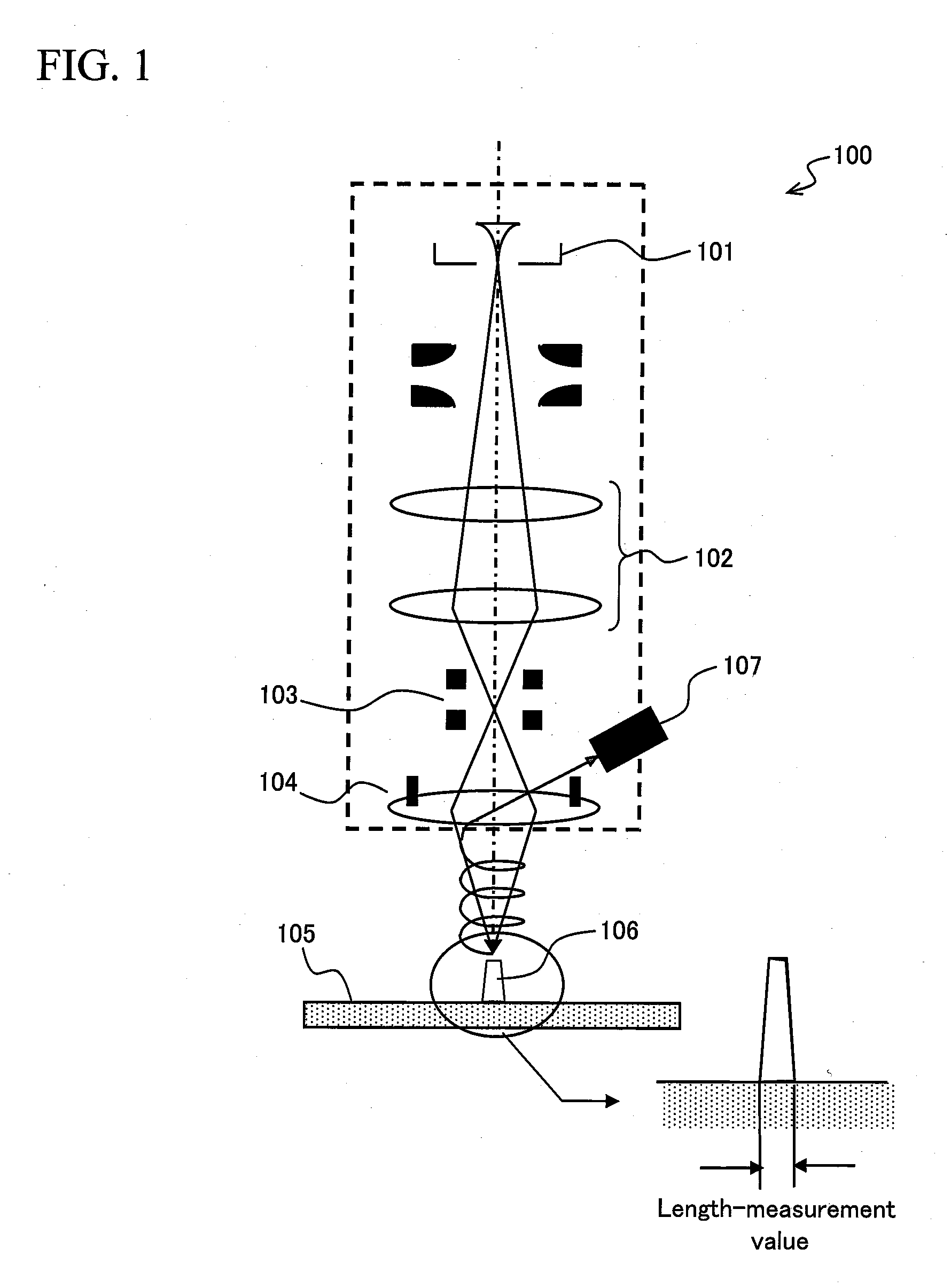
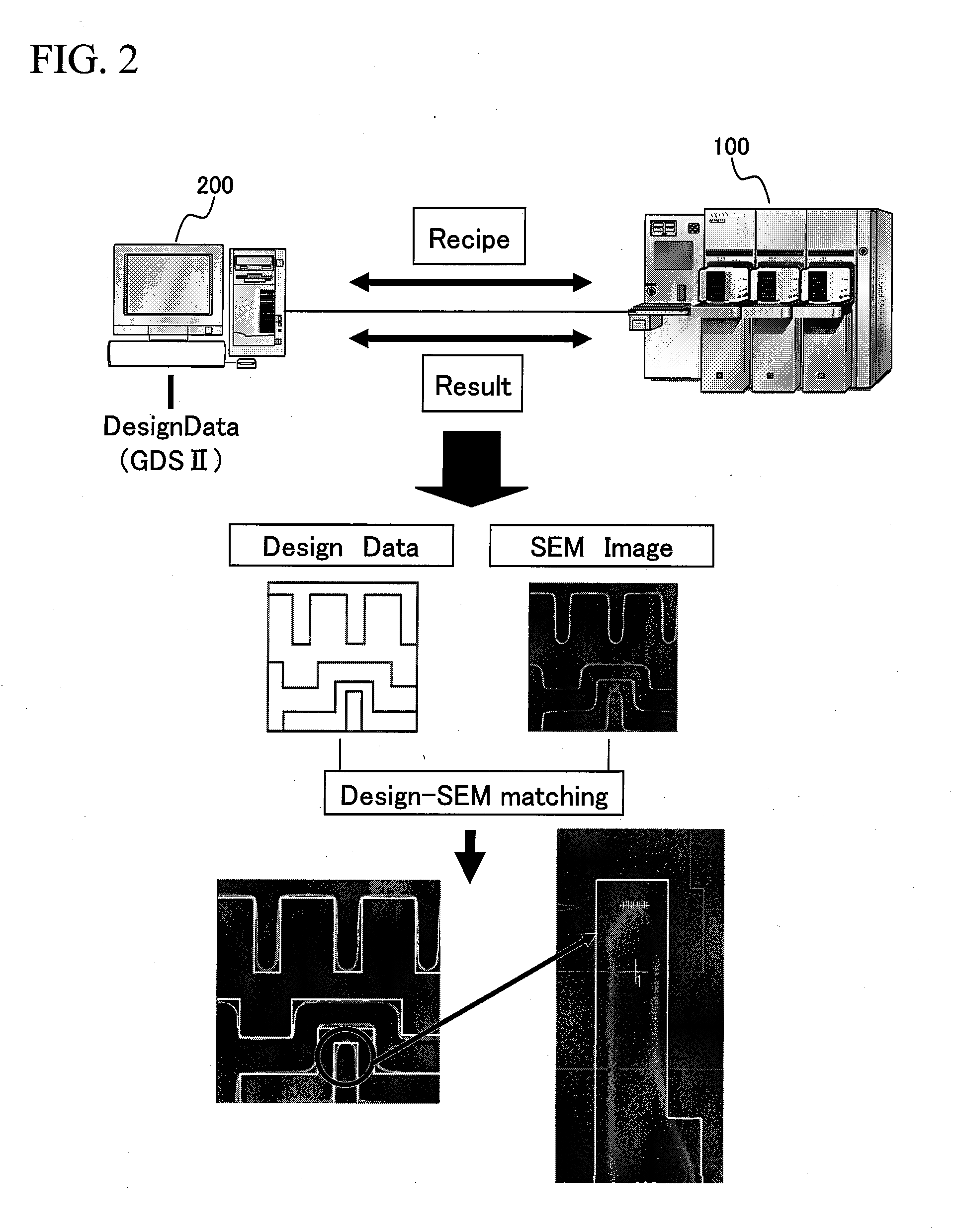
[0034]In a lithography step which is one of semiconductor manufacturing steps, the sizes of various patterns transferred onto a wafer are verified using a critical dimension scanning electron microscope (hereinafter referred to as the CD-SEM). FIG. 1 is a schematic view illustrating an approximate configuration of a CD-SEM 100.

[0035]In FIG. 1, the CD-SEM 100 is provided with an electron beam source 101 for emitting an electron beam, a convergence lens 102 for converging an electron beam, a deflection unit (deflection coil) 103 for deflecting an electron beam to scan a wafer (sample) 105, an objective lens 104 for irradiatin...


PUM


Abstract

A method capable of quantitatively evaluating two-dimensional patterns and a system to which the method is applied are provided. In the present invention, a reference coordinate system is set in order to convert pattern edge information (one-dimensional data) acquired by measurement using an existing critical dimension machine into coordinate data. Thus, a pattern is converted into coordinate information. Next, a function formula is determined from this coordinate information by approximate calculation and a pattern is represented by the mathematical expression y=f(x). Integrating y=f(x) in the reference coordinate used when calculating the coordinate data gives the area of the pattern, whereby it is possible to convert the coordinate data to two-dimensional data.

Description

BACKGROUND OF THE INVENTION[0001]1. Field of the Invention[0002]The present invention relates to a method of OPC model building, an information-processing apparatus, and a method of determining the process conditions of a semiconductor device. More particularly, the present invention relates to, for example, OPC modeling used in lithography requiring dissecting a pattern loyal to design data in ultra-microfabrication and in the field of semiconductor processes, and to the utilization of the OPC modeling.[0003]2. Background Art[0004]In the field of semiconductor processes, optical proximity correction (hereinafter referred as OPC) is carried out in some cases, in order to approximate a pattern on a wafer to a desired object (for example, CAD design). OPC is a technique especially effective in forming a microscopic pattern on a wafer.[0005]Methods of OPC include making a length measurement and a comparison of post-transfer pattern sizes using OPC-processed and non-OPC-processed mask p...

Claims


Application Information

Patent Timeline
IPC IPC(8): G06F17/50G03F1/36G03F1/68G03F1/84G03F1/86H01L21/027H01L21/82H01L21/822H01L27/04
CPCG03F1/144G03F7/70625G03F1/36G03F1/68
Inventor KIJIMA, MIHOKOYANG, KYOUNGMOSUKEGAWA, SHIGEKISUTANI, TAKUMICHI
Owner HITACHI HIGH-TECH CORP
Why Eureka
Try Eureka