Electrical interconnect structure and method

a technology of electrical interconnection and structure, applied in the direction of sustainable manufacturing/processing, final product manufacturing, semiconductor/solid-state device details, etc., can solve the problems of typical unreliable connection between structures and subject to failure, and achieve the effect of simple structur

Inactive Publication Date: 2008-10-16
ULTRATECH INT INC
View PDF9 Cites 20 Cited by
  • Summary
  • Abstract
  • Description
  • Claims
  • Application Information

AI Technical Summary

Benefits of technology

[0060]The present invention advantageously provides a simple structure and associated method for forming connections between structures.

Problems solved by technology

Connections between structures are typically unreliable and subject to failure.

Method used


Image

  • Electrical interconnect structure and method
  • Electrical interconnect structure and method
  • Electrical interconnect structure and method

Examples


Embodiment Construction

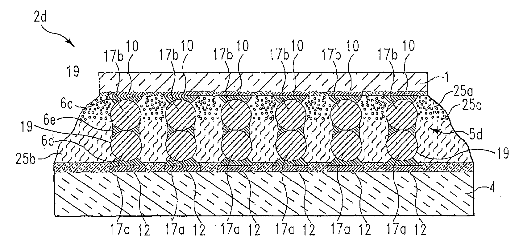
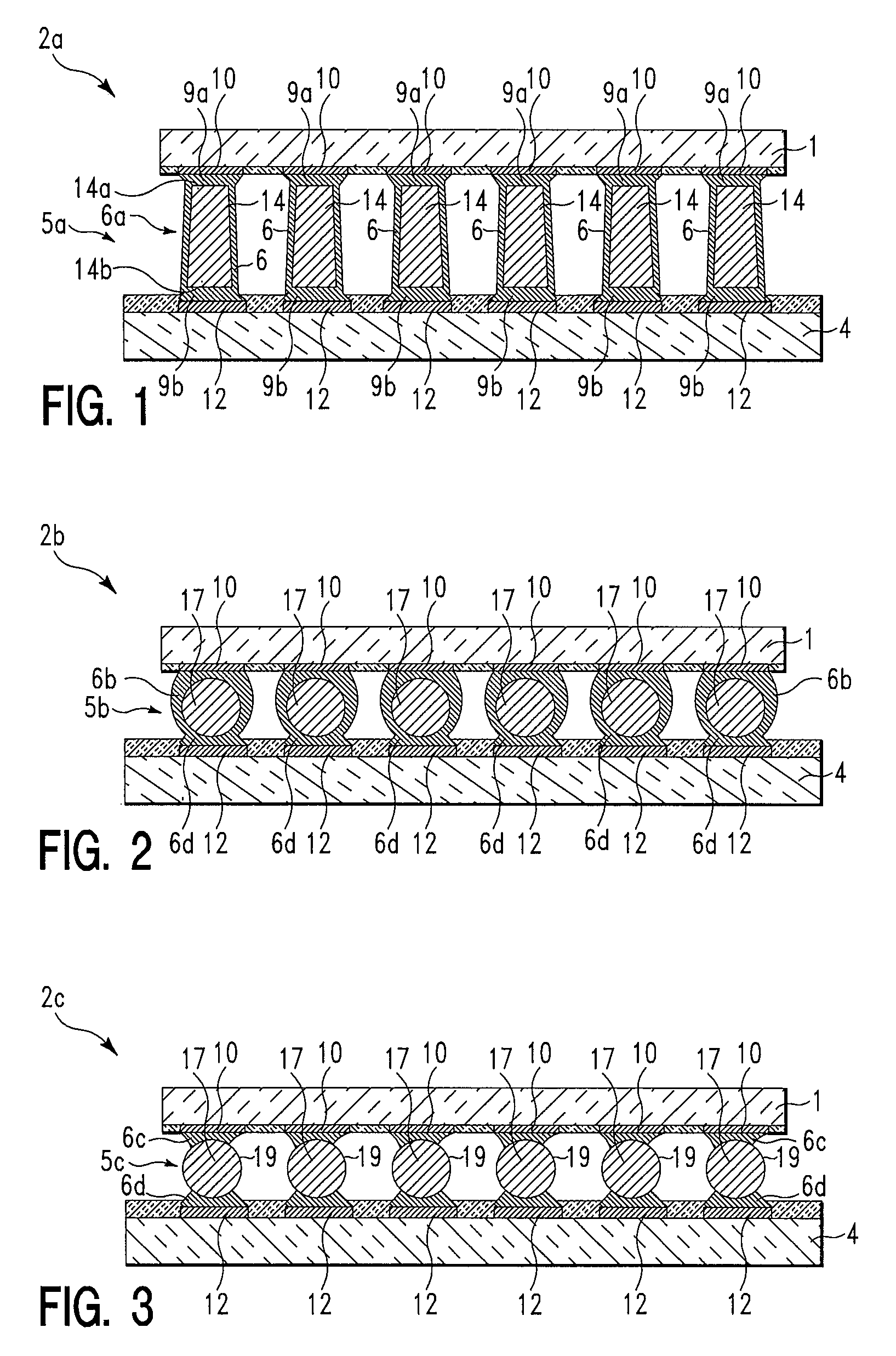
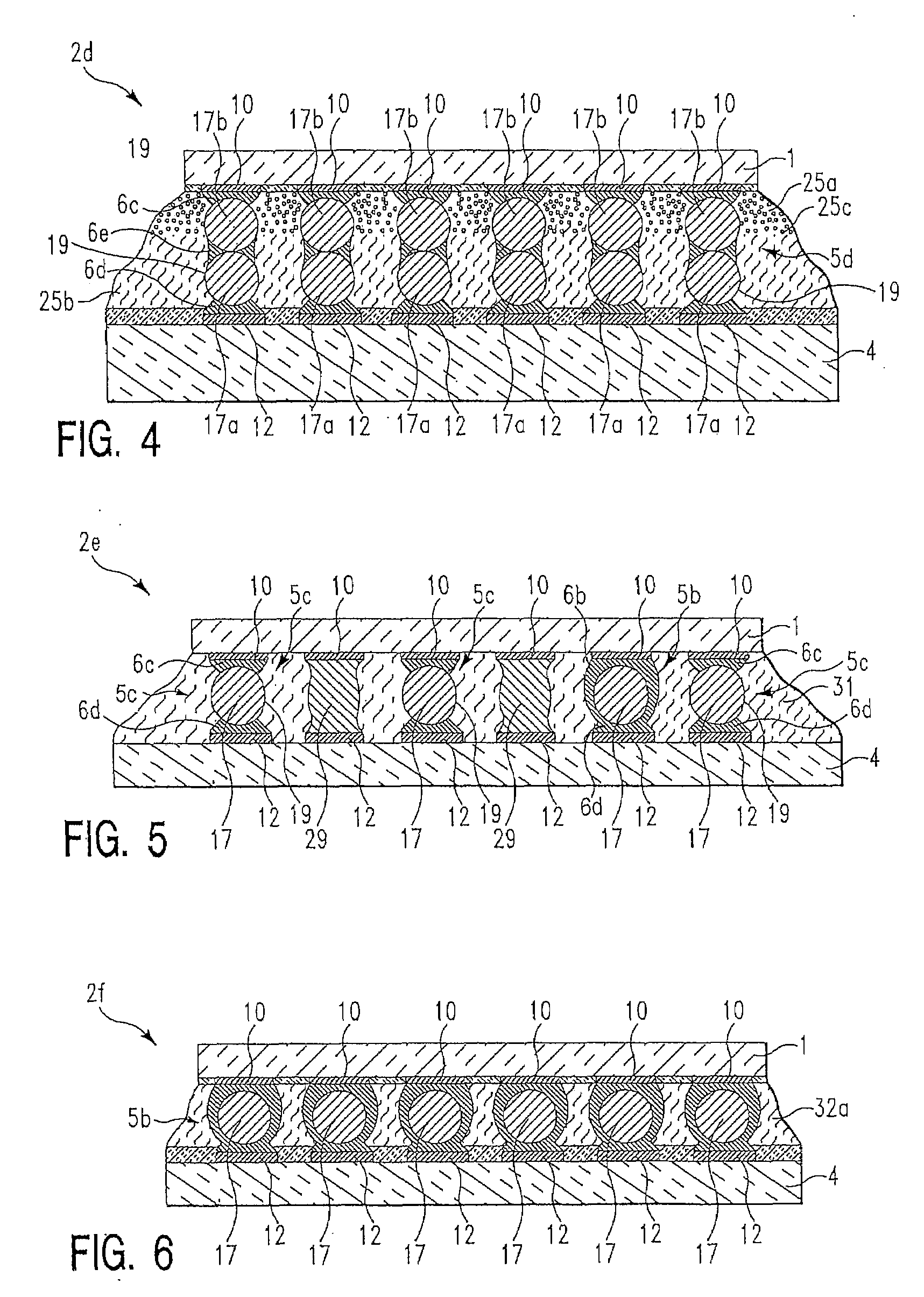
[0072]FIG. 1 illustrates a cross sectional view of an electrical structure 2a, in accordance with embodiments of the present invention. Electrical structure 2a comprises a substrate 1, a substrate 4, and a plurality of interconnect structures 5a. Substrate 1 comprises a plurality of electrically conductive pads 10. Each pad of electrically conductive pads 10 may be connected to wires or electrical components within substrate 1. Substrate 4 comprises a plurality of electrically conductive pads 12. Each pad of electrically conductive pads 12 may be connected to wires or electrical components within substrate 4. Substrate 1 may comprise, inter alia, a semiconductor device (e.g., an integrated circuit chip, a semiconductor wafer, etc), a chip carrier (organic or inorganic), a printed circuit board, etc. Substrate 4 may comprise, inter alia, a semiconductor device (e.g., an integrated circuit chip, a semiconductor wafer, etc), a chip carrier (organic or inorganic), a printed circuit boar...


PUM

PropertyMeasurementUnit
melting pointaaaaaaaaaa
diameteraaaaaaaaaa
diameteraaaaaaaaaa

Abstract

An electrical structure and method of forming. The electrical structure includes a first substrate comprising a first electrically conductive pad, a second substrate comprising a second electrically conductive pad, and an interconnect structure electrically and mechanically connecting the first electrically conductive pad to the second electrically conductive pad. The interconnect structure comprises a non-solder metallic core structure, a first solder structure, and a second solder structure. The first solder structure electrically and mechanically connects a first portion of the non-solder metallic core structure to the first electrically conductive pad. The second solder structure electrically and mechanically connects a second portion of the non-solder metallic core structure to the second electrically conductive pad.

Description

FIELD OF THE INVENTION[0001]The present invention relates to an electrical interconnect structure and associated method for forming an electrical interconnect structure.BACKGROUND OF THE INVENTION[0002]Connections between structures are typically unreliable and subject to failure. Accordingly, there exists a need in the art to overcome at least one of the deficiencies and limitations described herein above.SUMMARY OF THE INVENTION[0003]The present invention provides an electrical structure comprising:[0004]a first substrate comprising a first electrically conductive pad;[0005]a second substrate comprising a second electrically conductive pad; and[0006]an interconnect structure electrically and mechanically connecting said first electrically conductive pad to said second electrically conductive pad, wherein said interconnect structure comprises a non-solder metallic core structure, a first solder structure in direct mechanical contact with a first portion of said non-solder metallic ...

Claims


Application Information

Patent Timeline
Patent Type & Authority Applications(United States)
IPC IPC(8): H05K1/03H01K3/10
CPCH01L21/563H01L21/6835H01L24/11H01L24/12H01L24/16H01L24/28H01L24/31H01L24/73H01L24/81H01L24/94H01L2221/68377H01L2224/11003H01L2224/114H01L2224/116H01L2224/1308H01L2224/13082H01L2224/13111H01L2224/13144H01L2224/13147H01L2224/13155H01L2224/1357H01L2224/136H01L2224/16225H01L2224/274H01L2224/73203H01L2224/8121H01L2224/81815H01L2924/01004H01L2924/01005H01L2924/01029H01L2924/01033H01L2924/0105H01L2924/01079H01L2924/01082H01L2924/14H05K3/3436H05K2201/0379H05K2201/094H05K2201/10234H05K2201/10242H05K2201/10977H01L2924/0132H01L2924/00013H01L2924/01006H01L2924/01019H01L2924/014H01L2224/1131H01L2924/0133H01L2924/0001H01L24/27H01L2224/29111H01L2224/11822H01L2224/81191H01L2224/16H01L2224/11334Y10T29/49165H01L2924/00014H01L2224/45111H01L2924/01047H01L2224/13099H01L2924/01083H01L2924/00H01L2224/29099H01L24/05H01L24/13H01L24/17H01L24/29H01L24/32H01L2224/0554H01L2224/0557H01L2224/05571H01L2224/05573H01L2224/16238H01L2224/17051H01L2224/17505H01L2224/29082H01L2224/2919H01L2224/2929H01L2224/29299H01L2224/73104H01L2224/73204H01L2924/12042Y02P70/50H01L2224/05599H01L2224/0555H01L2224/0556H01L21/56H01L21/68H01L23/485
Inventor BUCHWALTER, STEPHEN LESLIEFURMAN, BRUCE K.GRUBER, PETER A.NAH, JAE-WOONGSHIH, DA-YUAN
Owner ULTRATECH INT INC
Why Eureka
Try Eureka