Electromigration-Resistant Flip-Chip Solder Joints

a flip-chip solder joint, electromigration-resistant technology, applied in semiconductor devices, semiconductor/solid-state device details, electrical apparatus, etc., can solve the problems of large electromigration voids at copper/solder joints, degrading etc., to reduce the formation of kirkendall voids, and improve the reliability of joints.

Inactive Publication Date: 2008-10-16
TEXAS INSTR INC
View PDF7 Cites 67 Cited by
  • Summary
  • Abstract
  • Description
  • Claims
  • Application Information

AI Technical Summary

Benefits of technology

[0006]The analysis of the solder contacts further revealed that an electrical current, which arrives at the contact from the high sheet resistance of the copper layer and has no chance to distribute to a lower resistance, remains crowded and causes large electromigration voids at the copper/solder joints. The electromigration driving force, in turn, enhances the Kirkendall void formation dramatically, further degrading the reliability of the joints.
[0007]The device structure according to the invention practically eliminates the copper diff

Problems solved by technology

The analysis of the solder contacts further revealed that an electrical current, which arrives at the contact from the high sheet resistance of the copper layer and has no chance to distribute to a lower resistance, remains

Method used


Image

  • Electromigration-Resistant Flip-Chip Solder Joints
  • Electromigration-Resistant Flip-Chip Solder Joints
  • Electromigration-Resistant Flip-Chip Solder Joints

Examples


Embodiment Construction

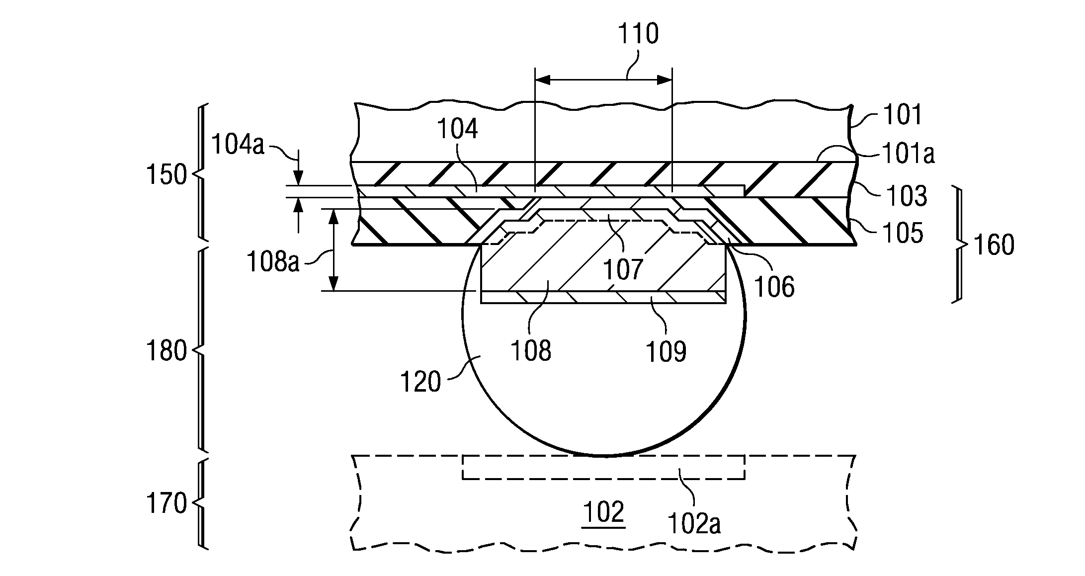
[0022]FIG. 1 illustrates an embodiment of the invention including a portion of a semiconductor chip 150, a structured contact pad 160 of the chip, and a solder ball 120 intended for electrical connection to external parts 170. The connection of contact pad 160 and solder 170 is reliable under the conditions of both accelerated stress tests and lifetime device operation, since the connection is structured to suppress electromigration as well as intermetallic formation and Kirkendall voiding.

[0023]In FIG. 1, the semiconductor material 101 has a surface 101a, which is covered by an interlevel dielectric layer (ILD) 103. The ILD may include silicon dioxide or mechanically weak materials of low dielectric constant such as silicon-containing hydrogen silsesquioxane. The thickness of layer 103 may vary widely (from 20 to 1000 nm), but is typically quite uniform across the wafer diameter. On the outward-facing surface of ILD layer 103 is an interconnect trace 104, which is a patterned inter...


PUM


Abstract

A semiconductor device contact structure practically eliminating the copper diffusion into the solder as well as the current crowding at the contact with the subsequent electromigration in the solder. A column-like electroplated copper stud (108) is on each contact pad. The stud is sized to provide low, uniform electrical resistance in order to spread the current from the contact to an approximately uniform, low density. Preferably, the stud height (108a) is at least ten times the thickness of the copper interconnect layer (104). Stud (108) is capped by an electroplated nickel layer (109) thick enough (preferably about 2 μm) to suppress copper diffusion from stud (108) into solder body (120), thus practically inhibiting intermetallic compound formation and Kirkendall voiding.

Description

FIELD OF THE INVENTION[0001]The present invention is related in general to the field of semiconductor devices and processes and more specifically to the structure and fabrication method of low cost, flip-chip solder joints, which are resistant against electromigration and void-causing intermetallic formation.DESCRIPTION OF THE RELATED ART[0002]In the continuing trend to miniaturize integrated circuits, the RC time constant of the metal layer interconnection between the active circuit elements increasingly dominates the achievable IC speed-power product. Consequently, the relatively high resistivity of the traditional interconnecting aluminum layer has in recent years been replaced by the lower resistivity of copper layer.[0003]In order to conserve silicon real estate, reduce device thickness and electrical resistance, semiconductor chips are increasingly assembled by flip-chip technology rather than wire bonding. In the flip-chip technology, it is common practice to interconnect the...

Claims


Application Information

Patent Timeline
IPC IPC(8): H01L21/31H01L21/44
CPCH01L24/11H01L2224/13099H01L2224/16H01L2924/01013H01L2924/01022H01L2924/01029H01L2924/01047H01L2924/01074H01L2924/01075H01L2924/01078H01L2924/01082H01L2924/01327H01L2924/14H01L2924/01019H01L2924/01024H01L2924/01033H01L2924/014H01L24/03H01L24/05H01L24/13H01L2224/0401H01L2224/05001H01L2224/05008H01L2224/05024H01L2224/05026H01L2224/05027H01L2224/0508H01L2224/05124H01L2224/05147H01L2224/05166H01L2224/05171H01L2224/05184H01L2224/05568H01L2224/05572H01L2224/05655H01L2224/13006H01L2224/16237H01L2924/181H01L2924/00H01L2924/00014H01L2924/013
Inventor ZHAO, JIE-HUAGUPTA, VIKASZENG, KEJUN
Owner TEXAS INSTR INC
Why Eureka
Try Eureka