Information Processing Device and Information Processing Method

a technology of information processing and information processing device, which is applied in the field of information processing device and information processing method, can solve the problems of implementation cost, implementation cost, power consumption and installation area, and the implementation cost of non-integer-ratio sampling rate conversion is generally great in the implementation cost in digital domain, and achieves the effect of low power consumption

Inactive Publication Date: 2008-10-16
SONY CORP
View PDF8 Cites 21 Cited by
  • Summary
  • Abstract
  • Description
  • Claims
  • Application Information

AI Technical Summary

Benefits of technology

[0037]Conversely, a system such as the decimation filter shown in FIG. 5 is equivalent to a two-stage configuration of SINC filters, so the implementation cost is very small. However, in the event of using SINC filters as an anti-aliasing filter, problems occur which necessitate consideration of property degradation, such as insufficient attenuation of aliasing, attenuation of the amplitude in the desired band, and so forth.
[0038]In order to minimize such effects, resampling is preferably performed at as high a frequency as possible, and the frequency range to be converted is set to or above the minimum desired band. Resampling at high frequency means that aliasing occurs further away from the desired band, which can be sufficiently attenuated by the SINC filters. That is to say, resampling at high frequency means that aliasing is not generated in the desired band, and the aliasing signals can be further attenuated using digital filters downstream. Also, this arrangement increases the notch frequency at the first-stage SINC filter, so the attenuation of the desired band is also smaller.
[0040]That is to say, implementation costs of the sampling rate conversion block can be reduced by using the decimation filter system shown in FIG. 5 at higher frequencies, but in the event that resampling is executed at high frequencies, the speed demanded of the upstream digital filter increases, so power consumption increases markedly.
[0041]That is to say, combining known methods only results in either the power consumption increasing due to the speed demanded of the upstream digital filter increasing, or the implementation cost of sampling rate conversion increasing due to the need to use a steep filter.
[0089]Thus, according to embodiments of the present invention, sampling rate conversion and filtering functionality can be realized, and particularly, sampling rate conversion and filtering functionality can be realized without raising power consumption by raising the speed demanded by digital filters, or using steep filters. Accordingly, low power consumption and capabilities to handle multiple standards can be realized while keeping the implementation costs of digital filters and sampling rate conversion.

Problems solved by technology

In the case of using the method described with reference to FIGS. 3 and 4, the clock frequency for realizing the lowest common multiple of 37.6875 MHz and 40 MHz is 24120 MHz, and when installation of the downstream digital filter is taken into consideration, this is impractical from the perspective of power consumption and installation area.
Thus, the implementation costs of non-integer-ratio sampling rate conversion is generally great in implementation cost in digital domain, and reduction in implementation costs can only come through accepting property degradation.
Conversely, a system such as the decimation filter shown in FIG. 5 is equivalent to a two-stage configuration of SINC filters, so the implementation cost is very small.
However, in the event of using SINC filters as an anti-aliasing filter, problems occur which necessitate consideration of property degradation, such as insufficient attenuation of aliasing, attenuation of the amplitude in the desired band, and so forth.

Method used


Image

  • Information Processing Device and Information Processing Method
  • Information Processing Device and Information Processing Method
  • Information Processing Device and Information Processing Method

Examples


Embodiment Construction

[0132]The embodiments of the present invention will be described below with reference to the diagrams.

[0133]A digital block having a sampling rate converting function wherein the present invention is applied is arranged to execute signal processing which is basically the same as a known case described with reference to FIG. 12 with a receiving device, without increasing the sampling frequency of the digital filter output, wherein a favorable receiving signal without aliasing can be obtained.

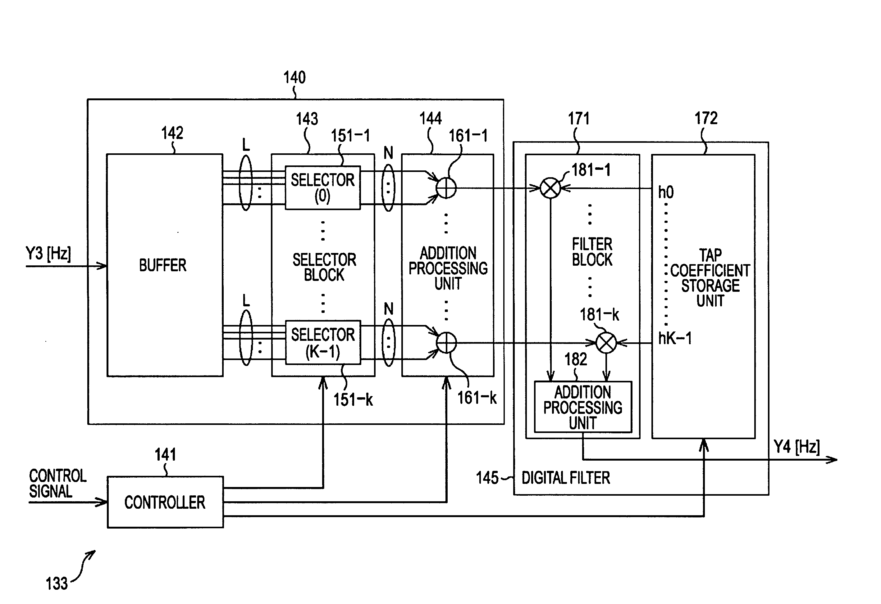
[0134]FIG. 13 is a block diagram showing the configuration of a digital block 111 in IEEE 802.11g OFDM mode wherein a decimation filter method is applied.

[0135]Note that the portions corresponding to the known case described with reference to FIG. 3 uses the same reference numerals, and the description thereof will be omitted as appropriate.

[0136]A SINC filter 51 receives an input signal with frequency Y1 MHz and executes moving average calculations. A decimator 131 reduces the sampling rate of t...


PUM


Abstract

An information processing device for processing reception signals converted into digital signals, includes: a first conversion unit for executing sampling rate conversion of each of the digital signals to be computed with each tap coefficient of a K'th-order FIR filter; a filter computing unit for executing computation processing of the K'th order FIR filter on K digital signals each of which have been subjected to sampling rate conversion by the first conversion unit; and a control unit for controlling sampling rate conversion of the digital signals by the first conversion unit, and the computation processing of the K'th order FIR filter by the filter computing unit.

Description

CROSS REFERENCES TO RELATED APPLICATIONS[0001]The present invention contains subject matter related to Japanese Patent Application JP 2006-330537 filed in the Japanese Patent Office on Dec. 7, 2006, the entire contents of which are incorporated herein by reference.BACKGROUND OF THE INVENTION[0002]1. Field of the Invention[0003]The present invention relates to an information processing device and information processing method, and particularly relates to an information processing device and information processing method suitable for using in cases of converting the sampling rate or oversampled reception signals.[0004]2. Description of the Related Art[0005]Semiconductor devices have become smaller and finer in recent years, and digital circuits have become capable of realizing lower power consumption and high speeds, with a smaller installation area as well. On the other hand, analog circuits cannot be expected to have reduction in installation area like digital circuits, and property...

Claims


Application Information

Patent Timeline
Patent Type & Authority Applications(United States)
IPC IPC(8): G06F17/10
CPCH03H17/0621H03H17/0685
Inventor BOSTAMAN, ANAS BIN MUHAMADYOKOSHIMA, HIDEKIABE, MASAYOSHIKONDO, YUYASANADA, YUKITOSHI
Owner SONY CORP
Why Eureka
Try Eureka