

Semiconductor structure having plural back-barrier layers for improved carrier confinement
a semiconductor structure and backbarrier technology, applied in the field of semiconductor structure and backbarrier layer to confine carriers, can solve the problems of degrading device performance, poor carrier transport properties of ingan carriers, and degrading device performance, so as to improve the confinement of carriers and high carrier energy
- Summary
- Abstract
- Description
- Claims
- Application Information
AI Technical Summary
Benefits of technology
Problems solved by technology
Method used
Image

Examples
Embodiment Construction
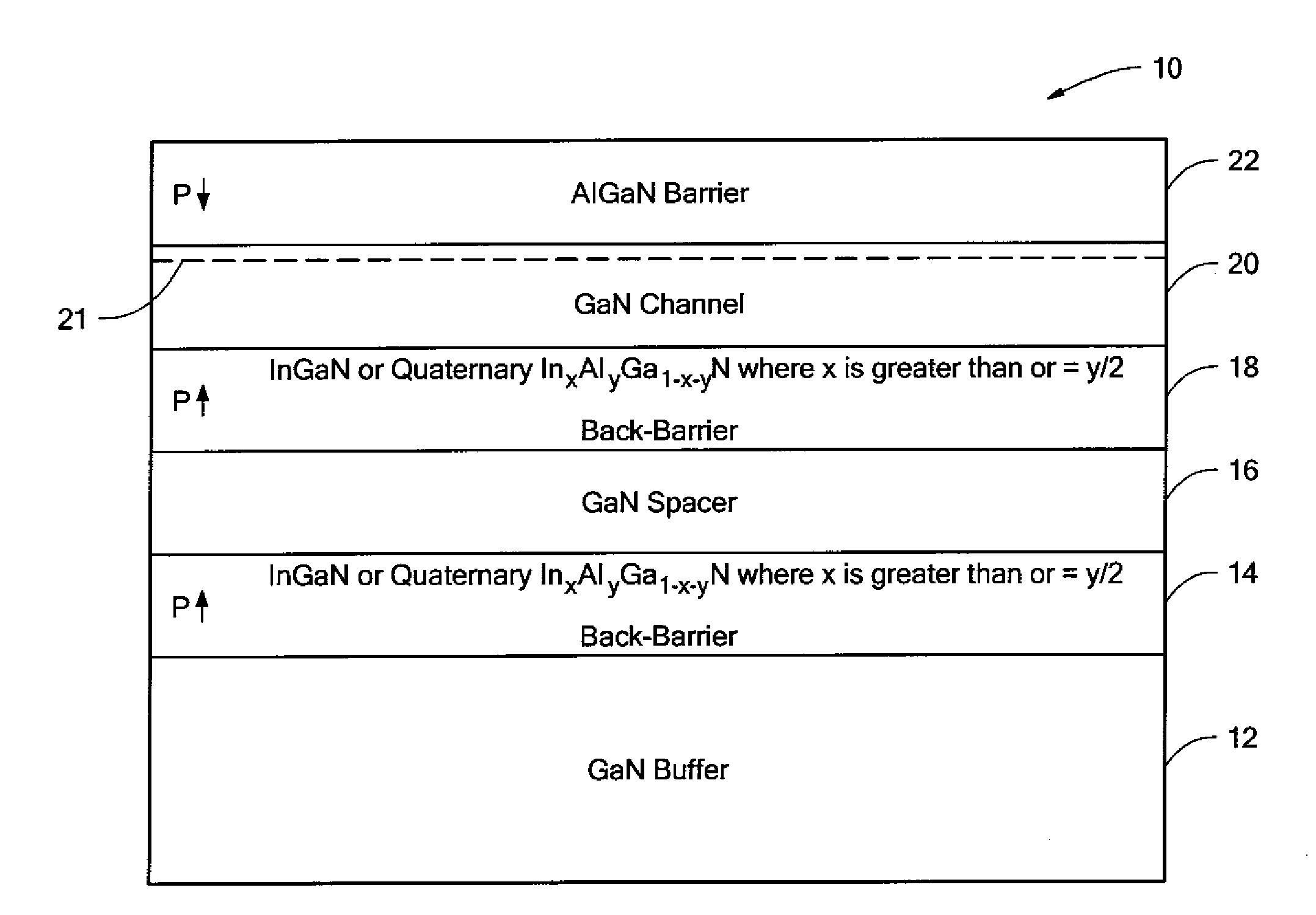
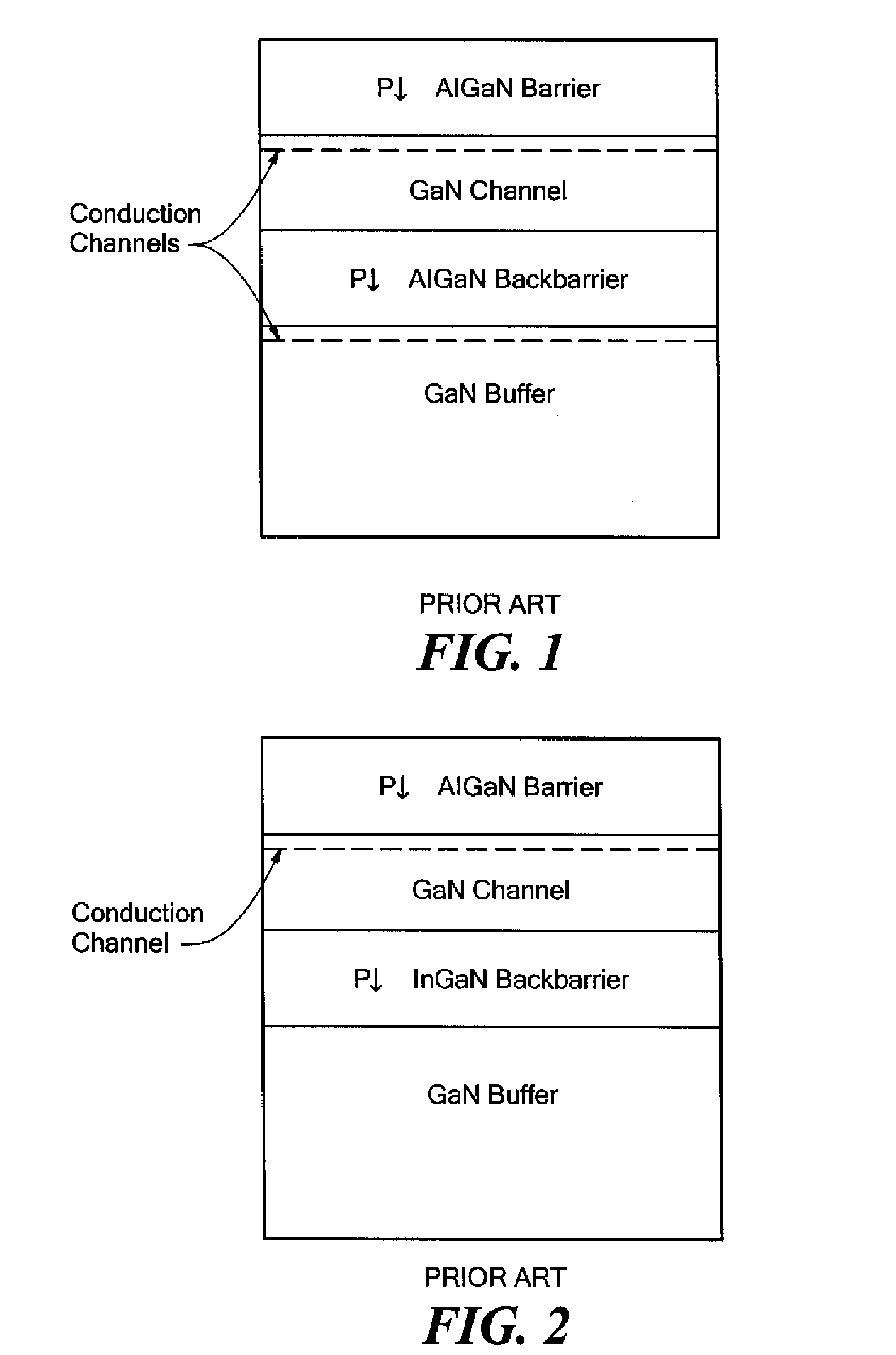
[0023]Referring now to FIG. 5, a semiconductor structure 10 is shown. Here the semiconductor structure 10 is suitable for a HEMT (i.e., High Electron Mobility Transistor) and includes: a GaN buffer layer 12; a plurality of, here two, InGaN back-barrier layers 14, 18 on the GaN buffer layer 12, with such pair of back-barrier layers 14, 18 being separated by a spacer layer 16, here a GaN spacer layer; a GaN channel layer 20; and an AlGaN barrier layer 22 on the channel layer.
[0024]Back-barrier layer 14 is here, for example, InGaN or quaternary InxAlyGa1-x-yN, where here x is greater than or equal to y / 2.
[0025]Back-barrier layer 18 is here, for example, InGaN or quaternary InxAlyGa1-x-yN, where here x is greater than or equal to 2y.
[0026]It is noted that one of the pair of back-barrier layers 14, 18 may be for example, InGaN, while the other one of the back-barrier layers 14, 18 may be of a different material, for example, quaternary InxAlyGa1-x-yN.
[0027]It is also noted that a heteroj...
PUM
 Abstract
Description
Claims
Application Information