Optically functional device

a functional device and optical waveguide technology, applied in the field of optical functional devices, can solve the problems of difficult to further reduce the driving voltage vl, device properties, etc., and achieve the effect of reducing the spot size of the optical waveguid

Active Publication Date: 2008-06-17
NGK INSULATORS LTD
View PDF11 Cites 7 Cited by
  • Summary
  • Abstract
  • Description
  • Claims
  • Application Information

AI Technical Summary

Benefits of technology

[0006]According to Japanese Patent applications 2002-330325 and 2003-136740, the thickness of a ferroelectric substrate forming an optical waveguide is made small to improve the intensity of electric field applied onto the substrate and to increase the effective electric field applied onto the optical waveguide. Vπ·L for driving the optical functional device can be thereby reduced.
[0007]It is effective for reducing the diameter of optical spot propagating in an optical waveguide, for further reducing Vπ·L for driving the optical functional device. The diameter of the optical spot propagating in the optical waveguide is, however, basically decided depending on the amount of an impurity such as titanium or proton normally diffused into the substrate and the processing temperature. If the confinement in the optical waveguide is made stronger to lower the diameter of the spot size, the propagation in the optical waveguide would be of multi-mode to result in problems of device properties. It has been thus considered to be difficult to further reduce the driving voltage Vπ·L by lowering the diameter of the optical spot.
[0008]An object of the present invention is to make it possible to lower the diameter of an optical spot propagating in an optical waveguide to reduce a driving voltage Vπ·L of an optical functional device.
[0021]That is, when the thickness Tsub of the ferroelectric thin layer 10 is sufficiently large, the equivalent refractive index Neff of the optical waveguide satisfies the relationship of Nfs<Neff<Np (In the case of cut-off state, however, it is satisfied the relationship of Neff<Nfs in the slab waveguide mode of the ferroelectric substrate). Np, Nfs, Nds and Nair represent the maximum value of the refractive index of the central and surface region of the impurity-diffused portion forming the optical waveguide, the refractive index of the non-diffused portion in the ferroelectric substrate 10, the refractive index of the dielectric substrate 5 and the refractive index of an air layer. As Tsub is lowered, Neff then begins to be lowered, so that the spot size of the optical waveguide is reduced in each of the depth and horizontal directions. This corresponds with the state of multi-mode in the direction of depth as described above. As Tsub is further lowered, the relationship of Neff / Nfs is then satisfied, so that the spot size of the optical waveguide is considerably reduced in each of the depth and horizontal directions.
[0023]When the waveguide is made multi-mode in the direction of depth of the ferroelectric thin layer 10, the confinement of light is strengthened in the horizontal direction of the optical waveguide, as well as the direction of the depth. The spot size of light is reduced in both of the depth direction “D” and width direction “W”. Particularly when Tsub is two times or lower than Dyo, the spot size of the fundamental mode is considerably reduced. It is proved that the driving voltage can be thereby considerably reduced in combination with the concentration of the electric lines of power near the surface region of the ferroelectric thin layer, and the present invention is made.

Problems solved by technology

If the confinement in the optical waveguide is made stronger to lower the diameter of the spot size, the propagation in the optical waveguide would be of multi-mode to result in problems of device properties.
It has been thus considered to be difficult to further reduce the driving voltage Vπ·L by lowering the diameter of the optical spot.

Method used


Image

  • Optically functional device
  • Optically functional device
  • Optically functional device

Examples


experiment 1

(Experiment 1)

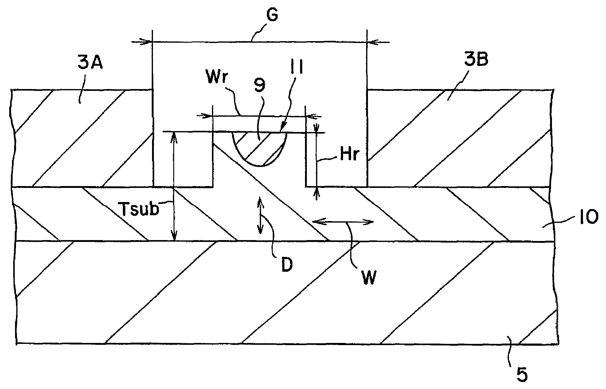
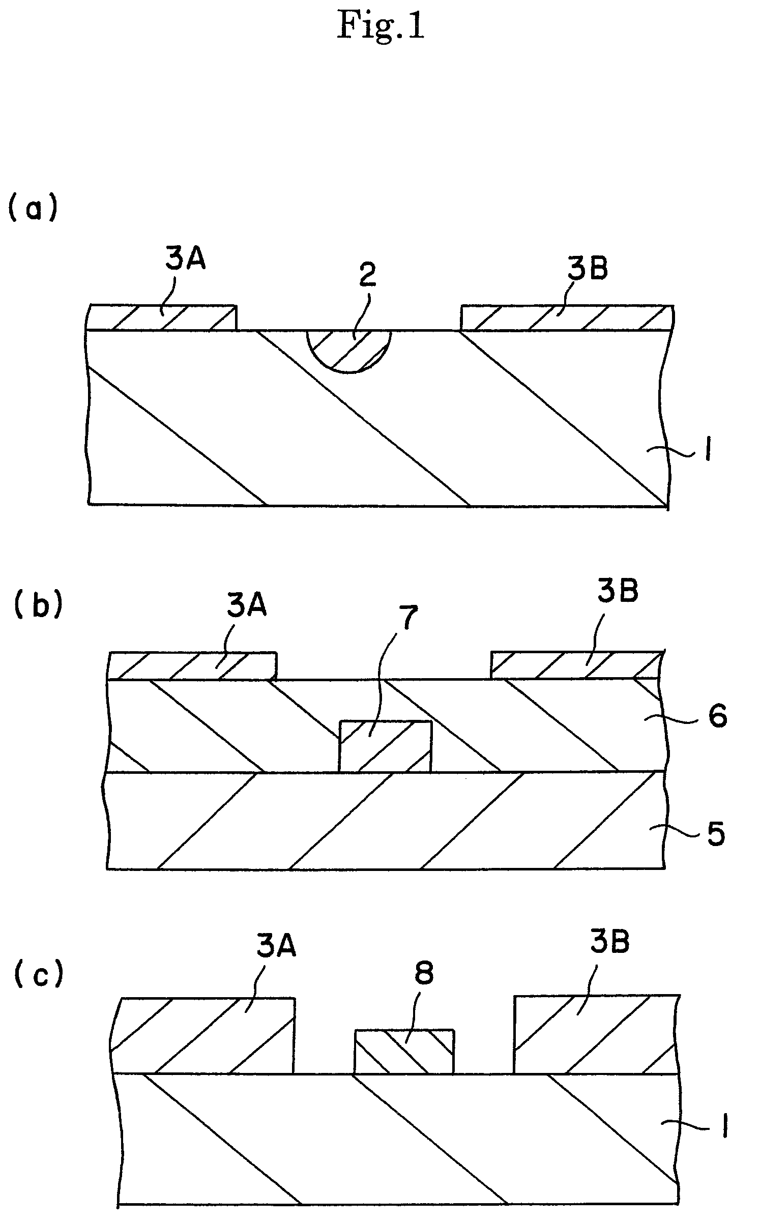
[0075]The optical modulator 1 shown in FIG. 2 (a) is produced. Specifically, a substrate composed of a 3-inch X-cut wafer (LiNbO3 single crystal) is used, and an optical waveguide 3 of Mach-Zehnder type is formed on the surface of the wafer, by titanium diffusion process and photolithography method. The thickness Tti of the titanium layer before the diffusion is made 0.08 μm and the width Wti is made 7 μm for making the confinement of light weaker compared with that in prior arts. Further, the treating temperature during the titanium diffusion is made 1050° C.

[0076]CPW electrode pattern is then formed by plating process. The gap “G” between the signal electrode 3B and ground electrode 3A is made 40, 30, 25, 20, 15, 10, 5 or 2 μm and the electrode length is made 35 mm. Then, for thinning, a dummy substrate is adhered to a polishing surface plate, and the modulator substrate is adhered thereon with a thermoplastic resin with the electrode face orientated downwardly. Furt...

experiment 2

(Experiment 2)

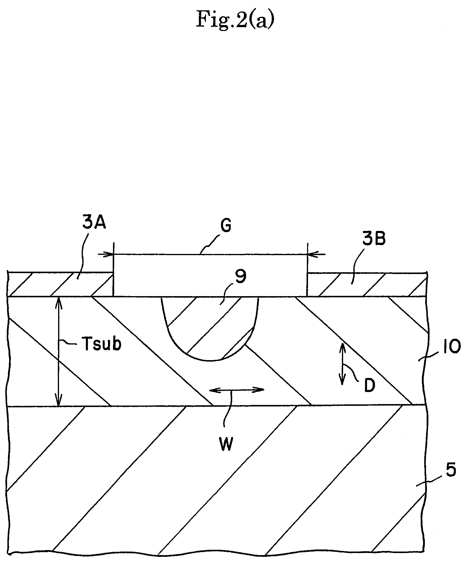
[0080]The optical modulation device of FIG. 2 (a) was produced by the same procedure as the experiment 1, under the conditions shown in each example of FIG. 9. However, the thickness Tti of titanium layer for the diffusion of titanium was made 0.06 μm, and the width Wti was made 5 μm. The thickness Tsub of the ferroelectric thin layer was changed in a range of 15 to 2 μm in addition to 500 μm. FIG. 9 shows the relationship of the electrode gap “G” and the driving voltage Vπ·L. According to the present example, the amount of titanium for the titanium diffusion was smaller than that used in the experiment 1, so that the confinement of light was relatively weak.

[0081]In the case that the substrate thickness was 500 μm, the spot size Dyo in the direction of depth of the propagating light was about 100 μm, and the equivalent refractive index Neff of the optical waveguide was 2.1371, which was slightly larger than the refractive index Nfs of 2.137 in the non-diffused portion...

experiment 3

(Experiment 3)

[0082]The optical modulating device was produced under the conditions shown in examples of FIG. 10, by the same procedure as the experiment 1. However, the thickness Tti and width Wti of the titanium layer for the titanium diffusion were changed as shown in FIG. 10. FIG. 10 shows the relationship between the optical spot size in the direction “W” of width and the substrate thickness Tsub. FIG. 11 shows the relationship between the optical spot size in the direction “D” of depth and the substrate thickness Tsub.

[0083]In the case that Tti is 0.08 μm and Wti is 7 μm, Dyo is 4 μm and Neff is 2.141 when Tsub is 500 μm. Although the optical spot size is not substantially changed at Tsub of 20 μm or larger, Neff is 2.141 or lower when Tsub is 10 μm or smaller and Neff is 2.137 when Tsub is 4 μm or smaller, so that the optical spot size is considerably decreased in the direction of depth. According to the case that Tti is 0.06 μm and Wti is 5 μm (Neff is 2.1371 and Dyo is 100 ...


PUM


Abstract

An optical functional device comprises a dielectric substrate 5, a ferroelectric thin layer 10 provided on the dielectric substrate 5 and comprising a material having electro-optical effect and an electrode 3A, 3B provided on the ferroelectric thin layer 10. A part of the ferroelectric thin layer 10 functions as a core 9 of the optical wave guide and the dielectric substrate functions as a clad for the optical waveguide. The optical waveguide 9 constitutes a multi-mode waveguide in the direction “D” of depth of the ferroelectric thin layer.

Description

FIELD OF THE INVENTION[0001]The present invention relates to an optical functional device.BACKGROUND OF THE INVENTION[0002]So-called multi-media industry has been developed and broad band communication has been increasingly demanded, so that it has been already applied an optical communication system operating at a speed higher than 10 Gb / s. Such system operating at even higher speed is expected. An LN optical modulator is applied as a device for modulating electrical signal of 10 Gb / s or higher (microwave signal) to light.[0003]It was invented a structure to satisfy velocity matching condition of microwave and light wave to realize wide-band modulation of an optical modulator, by lowering the thickness of an optical waveguide substrate (Japanese Patent publication No. 2002-169133A).DISCLOSURE OF THE INVENTION[0004]The applicant has disclosed that an adhesive layer having a substantially constant thickness is adhered onto the back face of a thin optical waveguide substrate having a ...

Claims


Application Information

Patent Timeline
Patent Type & Authority Patents(United States)
IPC IPC(8): G02B6/10
CPCG02F1/035G02F1/0508
Inventor MITOMI, OSAMUKONDO, JUNGOKONDO, ATSUOAOKI, KENJIEJIRI, TETSUYAIWATA, YUICHI
Owner NGK INSULATORS LTD
Why Eureka
Try Eureka