Method for producing at least one pad assembly on a support for the self-assembly of an integrated circuit chip on the support by the formation of a fluorinated material surrounding the pad and exposure of the pad and the fluorinated material to an ultraviolet treatment in the presence of ozone

a technology of integrated circuit chip and support, which is applied in the direction of sustainable manufacturing/processing, instruments, and final product manufacturing, can solve the problems of difficult to obtain a significant wettability difference between pads

Active Publication Date: 2015-10-08
COMMISSARIAT A LENERGIE ATOMIQUE ET AUX ENERGIES ALTERNATIVES +1
View PDF5 Cites 7 Cited by
  • Summary
  • Abstract
  • Description
  • Claims
  • Application Information

AI Technical Summary

Benefits of technology

[0014]An object of the present invention is to overcome all...

Problems solved by technology

However, with known methods, it may be difficult to obtain a ...

Method used


Image

  • Method for producing at least one pad assembly on a support for the self-assembly of an integrated circuit chip on the support by the formation of a fluorinated material surrounding the pad and exposure of the pad and the fluorinated material to an ultraviolet treatment in the presence of ozone
  • Method for producing at least one pad assembly on a support for the self-assembly of an integrated circuit chip on the support by the formation of a fluorinated material surrounding the pad and exposure of the pad and the fluorinated material to an ultraviolet treatment in the presence of ozone
  • Method for producing at least one pad assembly on a support for the self-assembly of an integrated circuit chip on the support by the formation of a fluorinated material surrounding the pad and exposure of the pad and the fluorinated material to an ultraviolet treatment in the presence of ozone

Examples


Embodiment Construction

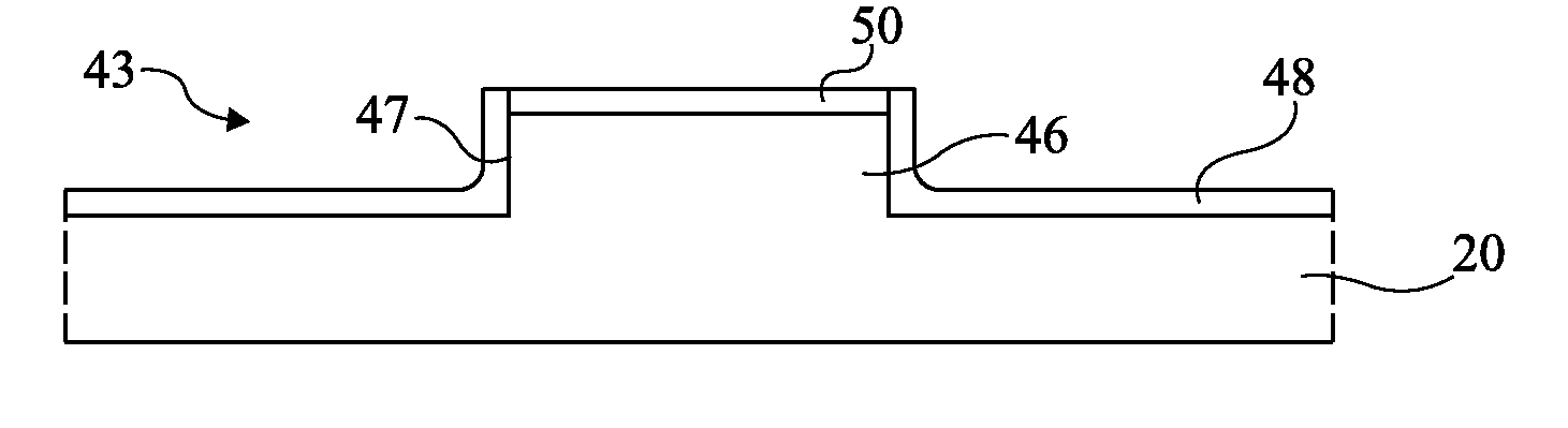
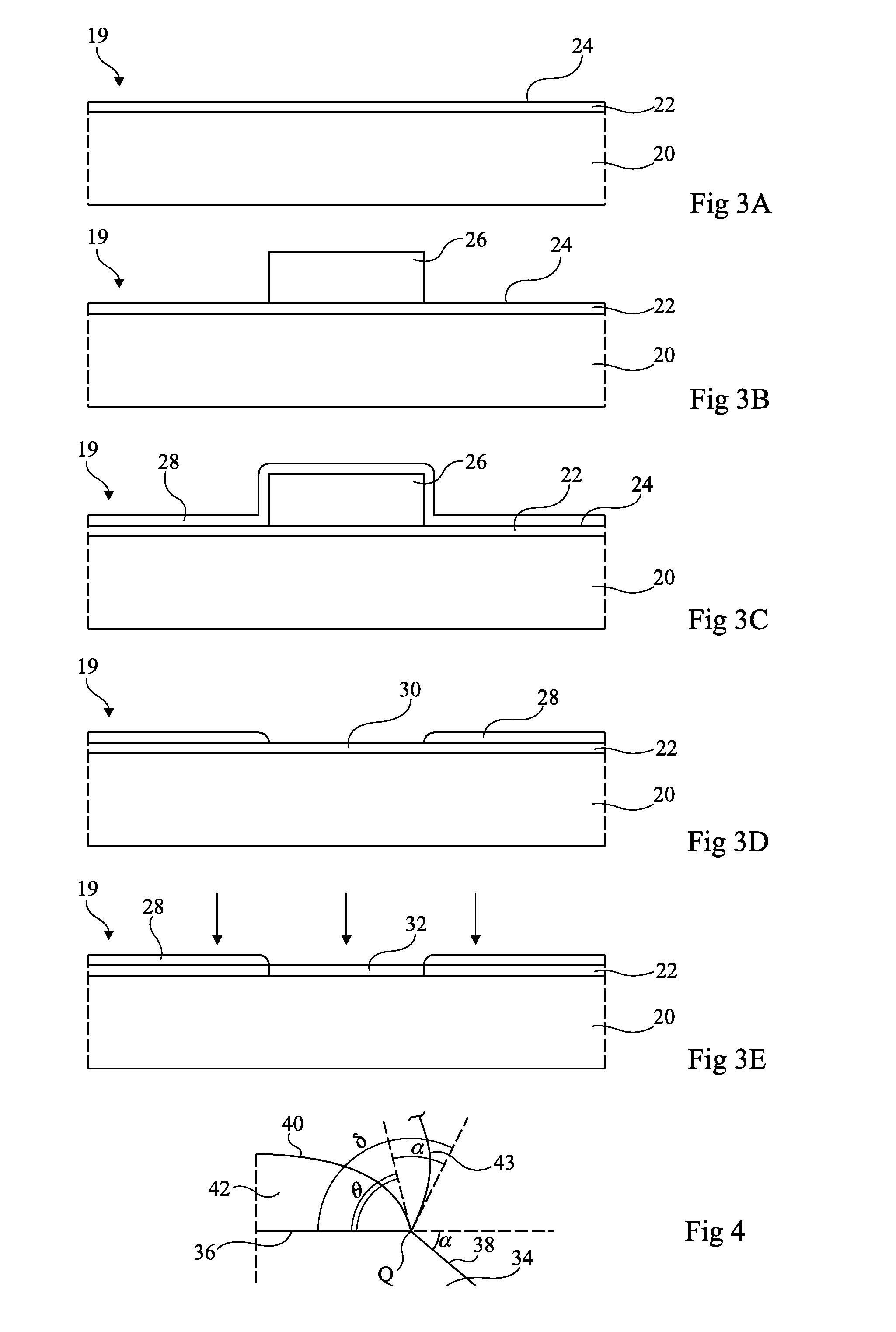
[0051]According to the present invention, the pads intended for the implementation of a self-assembly method are made of a material of high wettability, for which the static contact angle of a liquid drop on the material is smaller than or equal to 15°, preferably smaller than or equal to 10°, and preferably still smaller than or equal to 5°. Each pad is surrounded with a region of a material of low wettability, for which the static contact angle is greater than or equal to 100°, preferably greater than or equal to 110°, and preferably still greater than or equal to 115°.

[0052]According to the present invention, the pads of high wettability are formed after the regions of low wettability surrounding the pads. The method for manufacturing regions of low wettability thus causes no decrease in the wettability of the pads of high wettability. The high wettability of the pads is obtained by a processing under an ultraviolet radiation in the presence of ozone. For the method for manufactu...


PUM

PropertyMeasurementUnit
Angleaaaaaaaaaa
Angleaaaaaaaaaa
Angleaaaaaaaaaa

Abstract

A method for producing at least one pad assembly (32, 50) on a support (19, 43) for use in a method for self-assembling at least one element (10) on the support (19, 43), comprises fanning, on the support (19, 43), a layer (28, 48) of at least one fluorinated material around the location (30, 44) of the pad assembly (32, 50), the layer (28, 48) having a thickness greater than 10 nm. The layer (28, 48) and the location (30, 44) are exposed to an ultraviolet treatment in the presence of ozone to form the pad assembly (32, 50) at said location (30, 44), wherein a drop of liquid (16) having a static contact angle on the pad assembly (32, 50) less than or equal to 15°, after the exposure to the ultraviolet treatment, has a static contact angle on the layer (28, 48) greater than or equal to 100°.

Description

TECHNICAL FIELD[0001]The present disclosure relates to a method for manufacturing pads on a support for the implementation of a method of self-assembly of an electronic circuit on the support.DISCUSSION OF THE ART[0002]For certain applications, one or several electronic circuits, for example, integrated circuits, are bonded to a support. The support for example corresponds to another integrated circuit. The bonding is for example performed by molecular bonding or by thermocompression.[0003]Before bonding the integrated circuit to the support, it is necessary to properly arrange the integrated circuit with respect to the support. This may be done by a method of self-assembly of the integrated circuit on the support.[0004]FIGS. 1A to 1C are partial simplified cross-section views of the structures obtained at successive steps of an example of a method of self-assembly of an integrated circuit 10 on a support 11 and FIGS. 2A to 2C are respective cross-section views of the structures sho...

Claims


Application Information

Patent Timeline
IPC IPC(8): H01L23/00H01L23/14H01L21/311
CPCY10T428/24488Y10T428/24802H01L23/147H01L21/311H01L24/83H01L2224/08238H01L2224/80487H01L2224/08237H01L23/13H01L21/481H01L24/08H01L24/80H01L24/95H01L25/50H01L2224/80143H01L2224/83192H01L2224/95085H01L2224/95146H01L2224/80203H01L2224/08257H01L2224/08258H01L23/15H05K3/303H01L2224/80004Y02P70/50H01L2924/05442
Inventor DI CIOCCIO, LEAMERMOZ, SEBASTIENSANCHEZ, LOIC
Owner COMMISSARIAT A LENERGIE ATOMIQUE ET AUX ENERGIES ALTERNATIVES
Why Eureka
Try Eureka