Semiconductor structure for low parasitic gate capacitance

Active Publication Date: 2008-10-23
TWITTER INC
View PDF7 Cites 23 Cited by
  • Summary
  • Abstract
  • Description
  • Claims
  • Application Information

AI Technical Summary

Benefits of technology

[0026]According to a second embodiment of the present invention, a metal-

Problems solved by technology

Parasitic gate capacitance of a field effect transistor (FET) reduces the performance of the transistor by reducing the switching speed.
Particularly, high performance MOSFETs, in which contact vias to the source and drain regions are located close to the gate electrode to minimize the parasitic resistance of the source and drain region, suffer from high parasitic capacitance between the gate electrode and the contact vias du

Method used


Image

  • Semiconductor structure for low parasitic gate capacitance
  • Semiconductor structure for low parasitic gate capacitance
  • Semiconductor structure for low parasitic gate capacitance

Examples


first embodiment

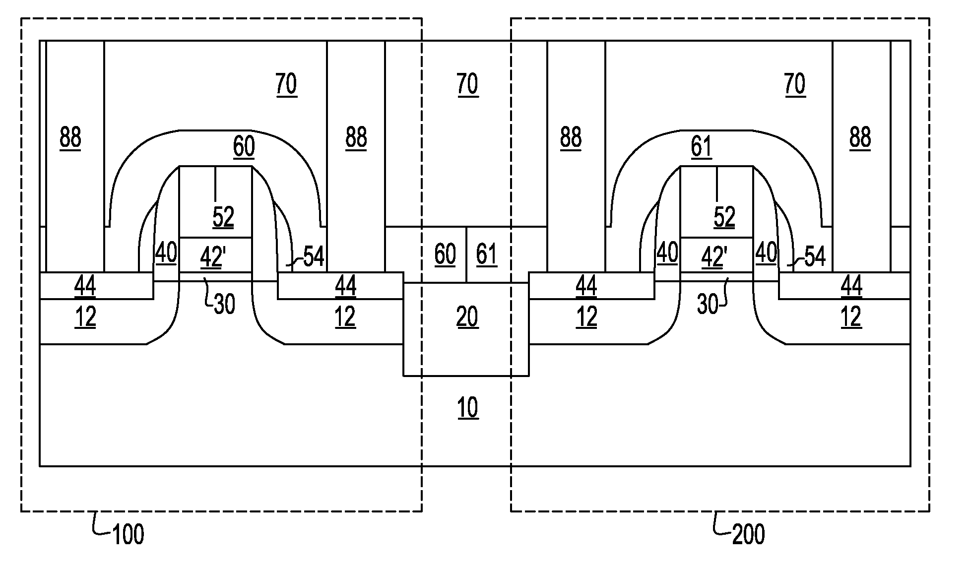
[0069]Referring to FIGS. 11A and 11B, the exemplary semiconductor structure according to the present invention is shown. The contact via holes (80, 90) are filled with metal to form contact vias (88, 98). The contact vias (88, 98) comprise substrate contact vias 88 and gate contact vias 98. The contact vias (88, 98) may be formed, for example, by chemical vapor deposition (CVD) of a metal film with reactant gases containing a metallic precursor gas such as tungsten hexafluoride (WF6). The portion of the metal film deposited above the MOL dielectric 70 may be removed by a blanket etch, chemical mechanical planarization (CMP), or a combination of both.

[0070]According to the first embodiment of the present invention, the low-k dielectric gate filler 52 directly contacts the inner sidewalls of the gate spacer 40 and the top surface of the gate silicide 42. The low-k dielectric gate filler 52 comprises a dielectric material with a dielectric constant of about 3.0 or less. The low-k secon...

fourth embodiment

[0079]According to the present invention, the cavity 92 directly contacts the inner sidewalls of the gate spacer 40 and the top surface of the gate silicide 42. The cavity 92 also contacts a bottom surface of either the first nitride liner 60 or the second nitride liner 61. At least one gate contact via 98 contacts the gate silicide 42 and plugs the corresponding at least one gate contact via hole 90. Therefore, the cavity 92 is enclosed by the inner sidewalls of the gate spacer 40, the top surface of the gate silicide 42, the bottom surface of either the first nitride liner 60 or the second nitride liner 61, and the at least one gate contact via 98. The top of the cavity 92 may be flush with the top of the gate spacer 40 or may be recessed relative to the top of the gate conductor 40.

[0080]The low-k secondary gate spacer 54 may be, or may not be, located directly on the gate spacer 40 and the source and drain silicide 44. The low-k secondary gate spacer 54 comprises a dielectric ma...


PUM


Abstract

A semiconductor structure provides lower parasitic capacitance between the gate electrode and contact vias while providing substantially the same level of stress applied by a nitride liner as conventional MOSFETs by reducing the height of the gate electrode and maintaining substantially the same height for the gate spacer. The nitride liner contacts only the outer sidewalls of the gate spacer, while not contacting inner sidewalls, or only a small area of the inner sidewalls of the gate spacer, therefore applying substantially the same level of stress to the channel of the MOSFET as conventional MOSFETs. The volume surrounded by the gate spacer and located above the gate electrode is either filled with a low-k dielectric material or occupied by a cavity having a dielectric constant of substantially 1.0. The reduced height of the gate electrode and the low-k dielectric gate filler or the cavity reduces the parasitic capacitance.

Description

FIELD OF THE INVENTION[0001]The present invention relates to semiconductor structures, and particularly to semiconductor structures with low parasitic gate capacitance and methods of manufacturing the same.BACKGROUND OF THE INVENTION[0002]Parasitic gate capacitance of a field effect transistor (FET) reduces the performance of the transistor by reducing the switching speed. Specifically, the capacitive coupling of a gate electrode to adjacent circuit components limits the rate at which the voltage of the gate electrode may be changed. The delay in the changes in the gate voltage due to the capacitive coupling with adjacent circuit components is then reflected in an increase in a turn-on time and a turn-off time of the field effect transistor.[0003]All transistors with a gate electrode, including junction field effect transistors (JFETs) and metal-oxide-semiconductor field effect transistors (MOSFETs), are prone to this type of parasitic capacitive coupling to adjacent circuit compone...

Claims


Application Information

Patent Timeline
IPC IPC(8): H01L21/285H01L21/336
CPCH01L21/28097H01L21/76814H01L21/7682H01L21/76832H01L21/76844H01L21/823807H01L21/823864H01L29/4975H01L29/517H01L29/66545H01L29/7843
Inventor HENSON, WILLIAM K.CHANG, PAUL CHUNG-MUHCHIDAMBARRAO, DURESETIDONATON, RICARDO A.LIU, YAOCHENGNARASIMHA, SHREESHTESSIER, AMANDA L.
Owner TWITTER INC
Why Eureka
Try Eureka