Unlock instant, AI-driven research and patent intelligence for your innovation.
Semiconductor device with improved pads
Active Publication Date: 2008-10-23
FUJITSU SEMICON MEMORY SOLUTION LTD
View PDF7 Cites 33 Cited by
Summary
Abstract
Description
Claims
Application Information
AI Technical Summary
This helps you quickly interpret patents by identifying the three key elements:
Problems solved by technology
Method used
Benefits of technology
Benefits of technology
[0025]These together with other aspects and advantages which will be subsequently apparent, reside in the details of construction and operation as more fully h
Problems solved by technology
It is well known that as moisture or water contents permeate a circuit region of a semiconductor integrated circuit device, the performance of the device is degraded.
When a probe needle is abutted on a pad during inspection, a crack may be formed in the pad.
However, the pad surface remains in an exposed state even after wire bonding so that moisture and hydrogen are likely to be permeated through the crack.
As the permeated moisture and hydrogen reach wirings or oxide, chemical reaction occurs and the performance of a semiconductor device is adversely affected.
Method used
Image
Click on the blue label to locate the original text in one second.
Reading with bidirectional positioning of images and text.
Examples
first embodiment
[0041]FIGS. 2A to 2S are cross sectional views and supplemental plan views of a semiconductor substrate illustrating main processes of a semiconductor device manufacture method according to the
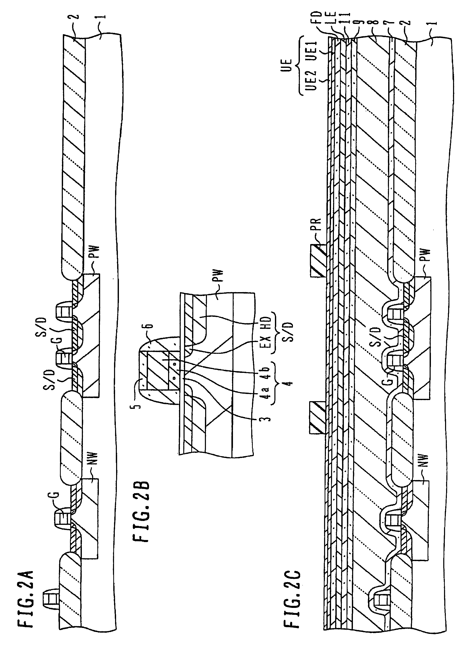
[0042]As shown in FIG. 2A, an isolation region 2 surrounding active regions necessary for circuit structures is formed in a semiconductor substrate 1, e.g., a silicon substrate, and an n-type well NW and a p-type well PW are formed in the active regions. In the structure shown, although the isolation region 2 is formed by local oxidation of silicon (LOCOS), it may be formed by shallow trench isolation (STI). A gate electrode G is formed above the active region, and source / drain regions S / D are formed in the active region on both sides of the gate electrode.
[0043]FIG. 2B is an enlarged cross sectional view of a transistor portion. A gate insulating film 3 of siliconoxide or the like is formed on the surface of the active region, and a gate electrode 4 made of a lamination of a polysilicon laye...
fourth embodiment
[0077]FIGS. 5A to 5D are schematic cross sectional views of a semiconductor device manufacture method according to the
[0078]As shown in FIG. 5A, processes similar to those of the first embodiment shown in FIGS. 2A to 2K are executed. After the ferroelectric capacitor is formed and covered with an alumina film 17, a silicon oxide film 18 and W plugs are formed, and thereafter the first metal wirings are formed and covered with an aluminum film 22 of 20 nm thick.
[0079]As shown in FIG. 5B, for example, a TEOS silicon oxide film 23 is formed on the alumina film 22 to a thickness of 2600 nm by CVD, and its surface is planarized by CMP. After the surface of the silicon oxide film 23 is nitridized, another TEOS silicon oxide film 24 is formed to a thickness of about 100 nm by CVD.
[0080]After the surface of the silicon oxide film 24 is nitridized, an alumina film 25 is formed to a thickness of about 250 nm by PVD such as sputtering. If necessary, thermal annealing is performed in an oxidizi...
fifth embodiment
[0083]FIGS. 6A to 6F show schematically the structure of a semiconductor device according to the
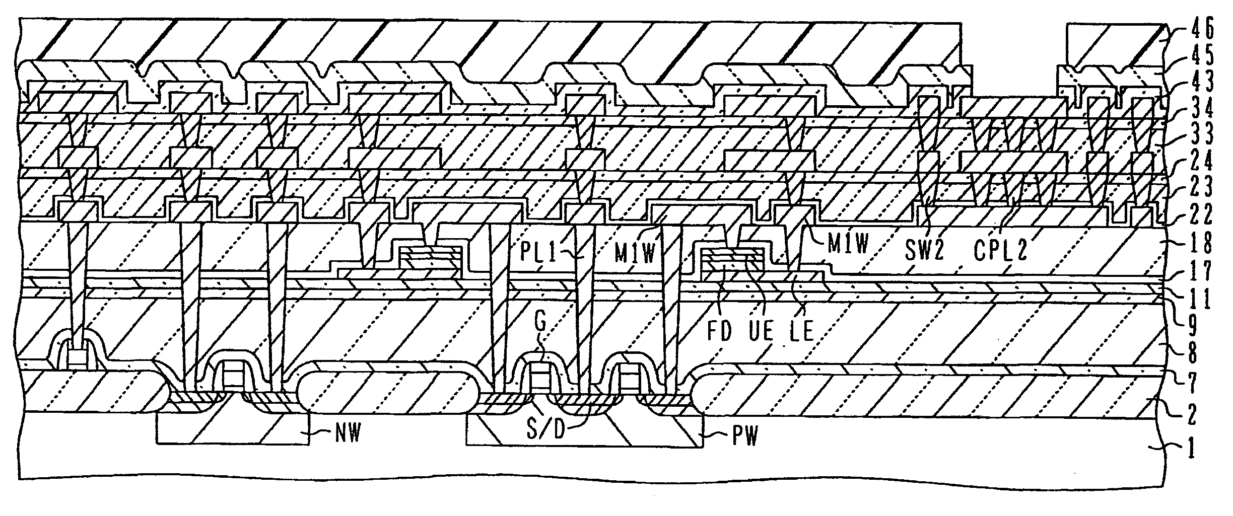
[0084]As shown in FIG. 6A, similar to the structure of the fourth embodiment shown in FIG. 4E, a sealing wall SW and a moisture resistant ring AHR1 are formed in the via conductor layer under the first metal wiring patterns M1W, and an alumina film 14 is inserted at the position crossing the via conductors and covered with a silicon oxide film 15. Similar to the structure of the fourth embodiment shown in FIG. 5D, alumina films 25 and 35 are inserted in the interlevel insulating film above the first metal wiring patterns M1W.
[0085]Further, also in the area inner than the bonding pad, an inner chip moisture resistant ring AHR2 having the structure similar to that of the chip moisture resistant ring AHR1 is formed. The inner chip moisture resistant ring AHR2 is cut off in an area where a bonding pad lead wiring exists.
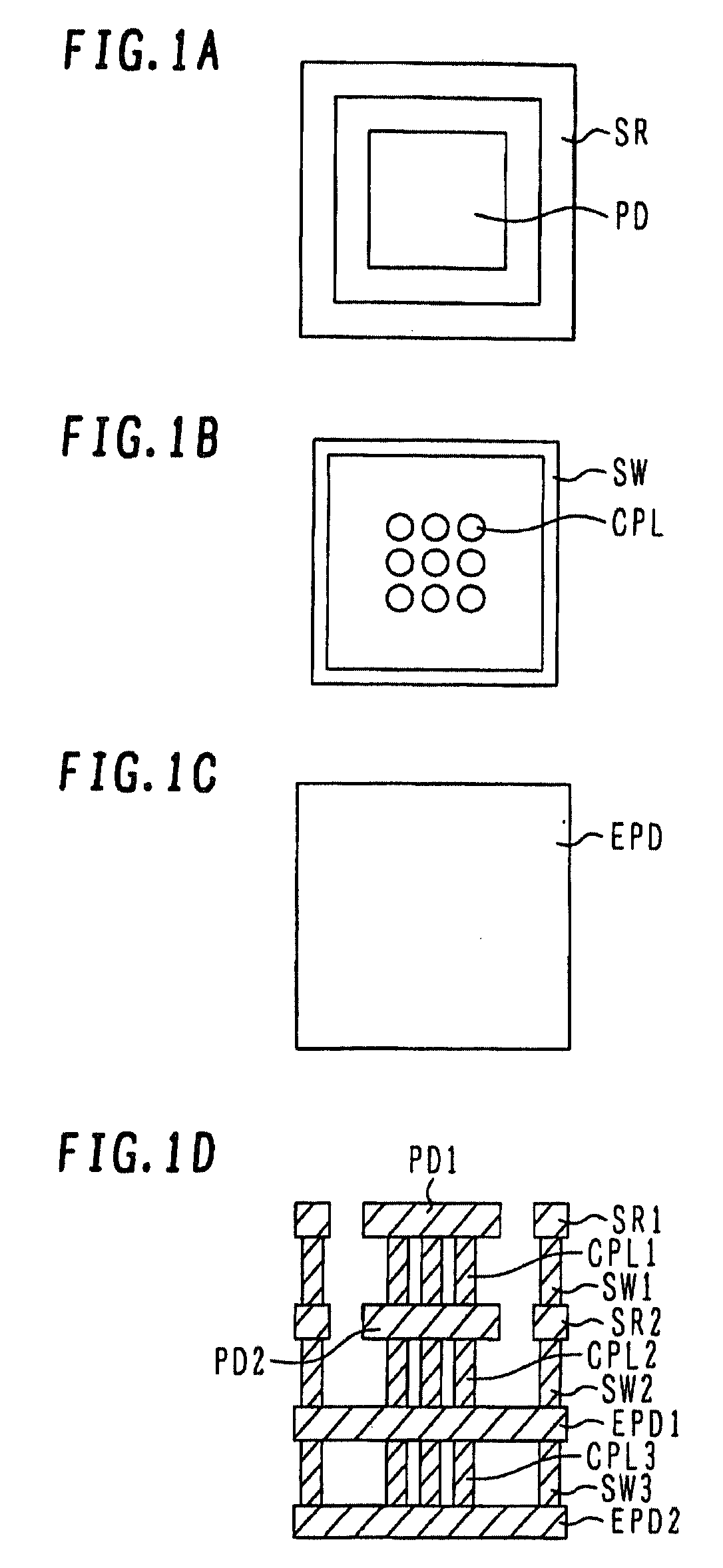
[0086]FIG. 6B is a schematic plan view of the bonding pad structure of th...
PUM
Abstract
A semiconductor device has: a circuit portion having semiconductor elements formed on a semiconductor substrate; insulating lamination formed above the semiconductor substrate and covering the circuit portion; a multilevel wiring structure formed in the insulating lamination and including wiring patterns and via conductors; and a pad electrode structure formed above the semiconductor substrate and connected to the multilevel wiring structure. The pad electrode structure includes pad wiring patterns and pad via conductors interconnecting the pad wiring patterns, the uppermost pad wiring pattern includes a pad pattern and a sealing pattern surrounding the pad pattern in a loop shape. Another pad wiring pattern has continuous extended pad pattern of a size overlapping the sealing pattern. The pad via conductors include a plurality of columnar via conductors disposed in register with the pad pattern and a loop-shaped wall portion disposed in register with the sealing pattern.
Description
CROSS REFERENCE TO RELATED APPLICATION[0001]This application is a continuation application of international application, PCT / JP2005 / 023965, the entire contents of which are incorporated herein by reference.BACKGROUND[0002]A) Field[0003]The embodiments discussed herein are directed to a semiconductor device, which may relate to a semiconductor device having pads for connection to an external circuit and for inspection.[0004]B) Description of the Related Art[0005]It is well known that as moisture or water contents permeate a circuit region of a semiconductor integrated circuit device, the performance of the device is degraded. In order to shield moisture permeating from a chip outer periphery, a moisture resistant ring for shielding moisture is formed along the chip outer periphery.[0006]JP-A-2002-270608 (applicant: Fujitsu Limited) proposes a semiconductor device having a damascene wiring structure burying wiring patterns and via conductors in an interlevel insulating film, in which ...
Claims
Application Information
Patent Timeline
Application Date:The date an application was filed.
Publication Date:The date a patent or application was officially published.
First Publication Date:The earliest publication date of a patent with the same application number.
Issue Date:Publication date of the patent grant document.
PCT Entry Date:The Entry date of PCT National Phase.
Estimated Expiry Date:The statutory expiry date of a patent right according to the Patent Law, and it is the longest term of protection that the patent right can achieve without the termination of the patent right due to other reasons(Term extension factor has been taken into account ).
Invalid Date:Actual expiry date is based on effective date or publication date of legal transaction data of invalid patent.



