Eureka AIR delivers breakthrough ideas for toughest innovation challenges, trusted by R&D personnel around the world.

Method and Apparatus for Small Die Low Power System-on-Chip Design with Intelligent Power Supply Chip

a low-power, intelligent power supply technology, applied in the direction of individual semiconductor device testing, program control, instruments, etc., can solve the problems of long circuit design time, large silicon area, high power consumption, etc., and achieve the effect of improving design time, reducing power consumption, and small circuit footprin

Active Publication Date: 2008-10-23
DIALOG SEMICONDUCTOR INC
View PDF21 Cites 8 Cited by
  • Summary
  • Abstract
  • Description
  • Claims
  • Application Information

AI Technical Summary

Benefits of technology

[0009]The invention results in improved design times, a smaller circuit footprint, lower power consumption, reduced costs, and the removal of the worst-case scenarios.

Problems solved by technology

However the three most important constraints are the process corner, temperature, and power supply.
Without the integration of the power supply design, several problems arise in SOC production, including long circuit design times, large silicon area, high power consumption and high material and labor costs.
Additionally, this separate design approach gives rise to the worst-speed and worst-power cases.
From the worst-speed case the following problems arise: a lower supply voltage head room and slower transistor speed, a larger transistor W / L ratio is used to compensate, and a higher die cost.
This case creates the following problems: a larger current from higher transistor speed and higher supply voltage, a higher thermal coefficient package or heat sink used, and a higher package cost.

Method used


Image

  • Method and Apparatus for Small Die Low Power System-on-Chip Design with Intelligent Power Supply Chip
  • Method and Apparatus for Small Die Low Power System-on-Chip Design with Intelligent Power Supply Chip
  • Method and Apparatus for Small Die Low Power System-on-Chip Design with Intelligent Power Supply Chip

Examples


Embodiment Construction

[0014]Reference is made in detail to the preferred embodiments of the invention. While the invention is described in conjunction with the preferred embodiments, the invention is not intended to be limited by these preferred embodiments. On the contrary, the invention is intended to cover alternatives, modifications and equivalents, which may be included within the spirit and scope of the invention as defined by the appended claims. Furthermore, in the following detailed description of the invention, numerous specific details are set forth in order to provide a thorough understanding of the invention. However, the invention may be practiced without these specific details. In other instances, software or database applications, network systems, and electronic or optical circuits have not been described in detail so that aspects of the invention will not be obscured.

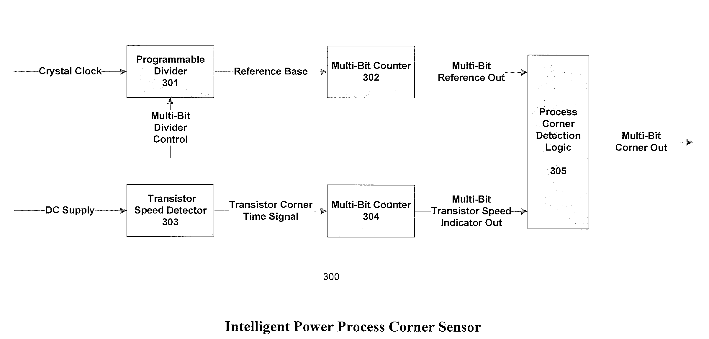
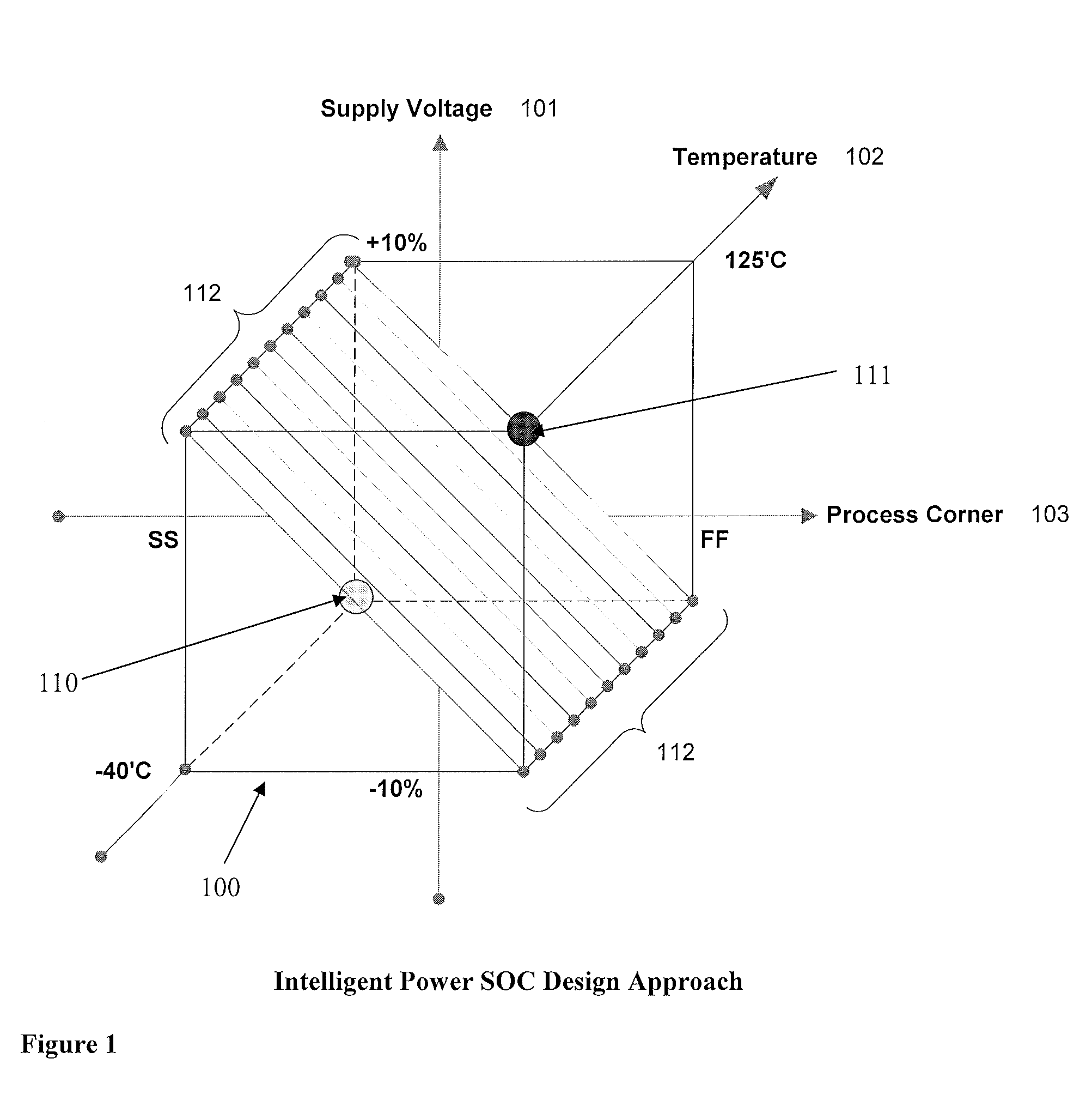
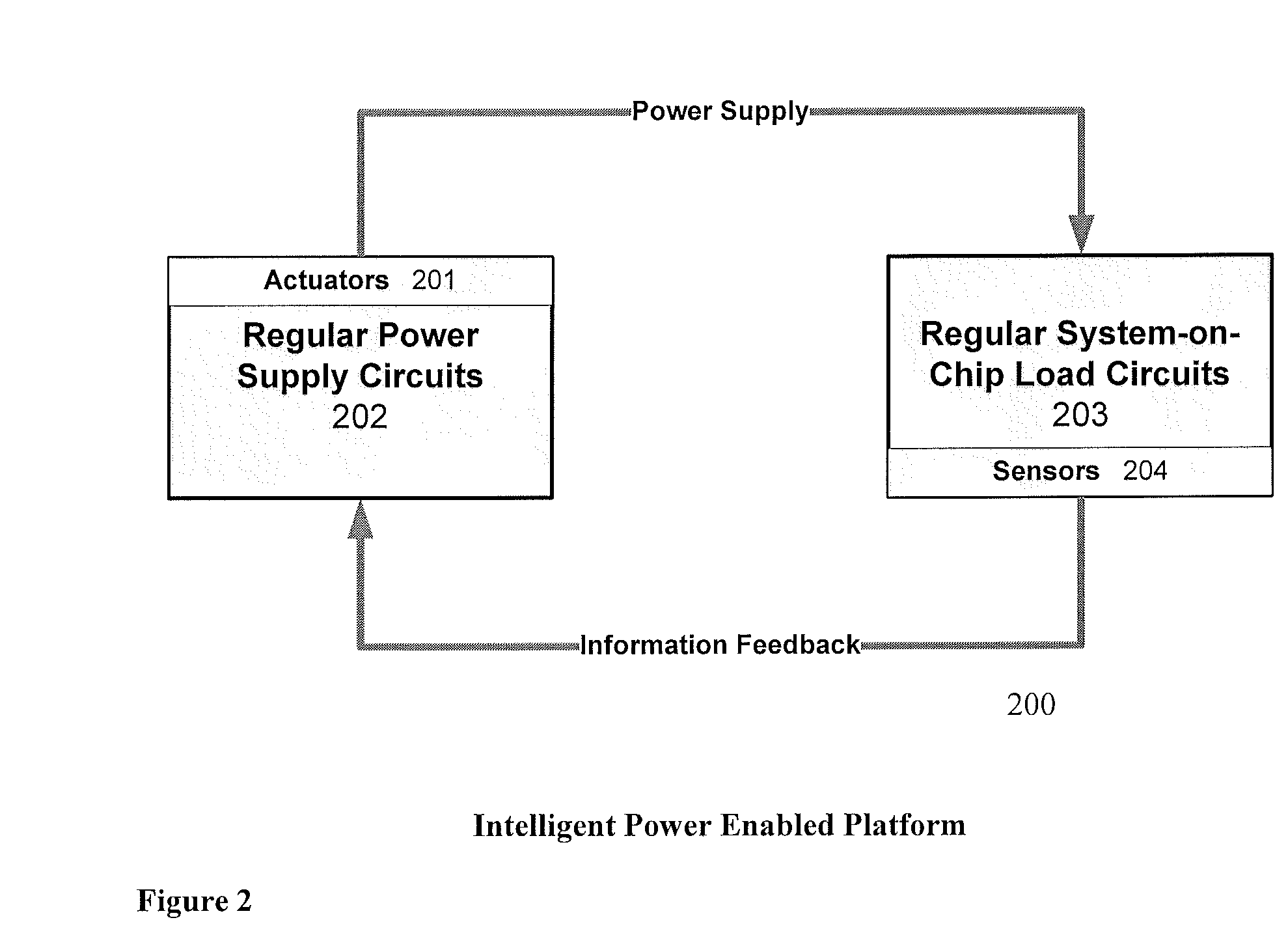
[0015]FIG. 1 is a simplified diagram that illustrates the design corners 100 of the intelligent power SOC design approach ...


PUM


Abstract

A method and system of system-on-chip design that provides the benefits of reduced design time, a smaller die size, lower power consumption, and reduced costs in chip design and production. The process seeks to remove the worst performance and worst power case scenarios from the design and application phases. This is accomplished by planning the power supply voltage in the design phase along with its tolerance with process corner and temperature combinations. The established plan is then applied with communications between power supply integrated circuits and load system-on-chip.

Description

FIELD OF INVENTION[0001]This invention pertains to circuit design methodology relating to power consumption.BACKGROUND[0002]There are many factors to consider in SOC design. However the three most important constraints are the process corner, temperature, and power supply. The conventional SOC design methods use electronic design automation tools which assume a power supply voltage on certain combination or range of supply voltage while working with changing process corner and temperature parameters.[0003]The power supply design is done independently from the SOC process corner and temperature design process. Without the integration of the power supply design, several problems arise in SOC production, including long circuit design times, large silicon area, high power consumption and high material and labor costs.[0004]Additionally, this separate design approach gives rise to the worst-speed and worst-power cases. The worst-speed case or performance bottleneck occurs at the lowest s...

Claims


Application Information

Patent Timeline
IPC IPC(8): G06F17/50G01R31/26
CPCG06F17/5045G06F2217/78G06F30/30G06F2119/06
Inventor JIN, XUECHENGMALININ, ANDREY B.KESTERSON, JOHN W.
Owner DIALOG SEMICONDUCTOR INC
Why Eureka
Eureka Blog
Learn More