Device structure and manufacturing method using HDP deposited source-body implant block

Active Publication Date: 2008-10-30
ALPHA & OMEGA SEMICON LTD
View PDF16 Cites 71 Cited by
  • Summary
  • Abstract
  • Description
  • Claims
  • Application Information

AI Technical Summary

Benefits of technology

[0006]It is therefore an aspect of the present invention to provide a new and improved semiconductor power device by applying a new manufacturing method that is able to control plasma deposition at target areas. This new HDP deposition method is able to simplify the

Problems solved by technology

However, in order to form a thick oxide layer on the trench bottom or a split gate with split and mutually insulated bottom and top gate segment in the trench typically require additional processing steps.
These additional proc

Method used


Image

  • Device structure and manufacturing method using HDP deposited source-body implant block
  • Device structure and manufacturing method using HDP deposited source-body implant block
  • Device structure and manufacturing method using HDP deposited source-body implant block

Examples


Embodiment Construction

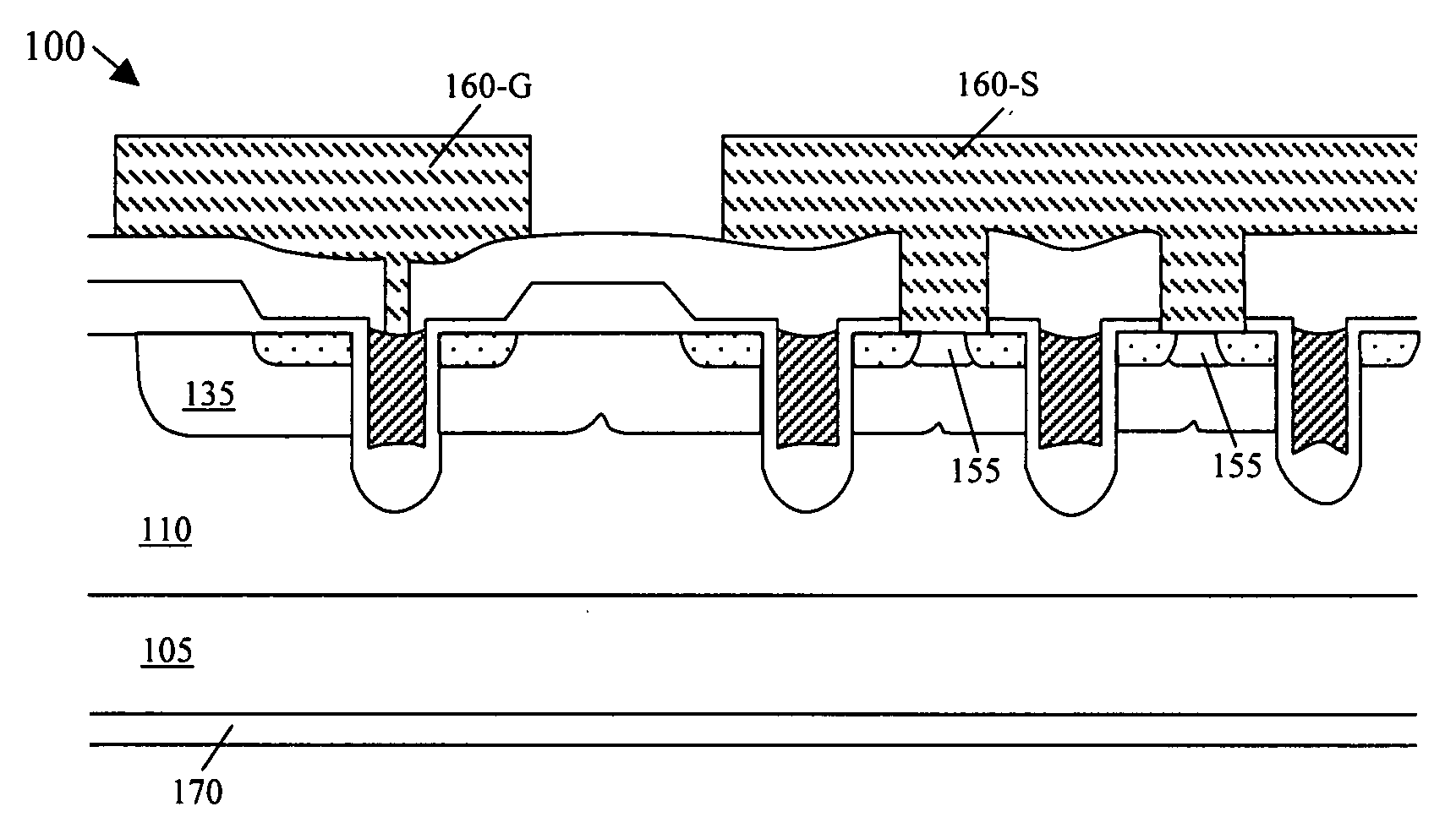
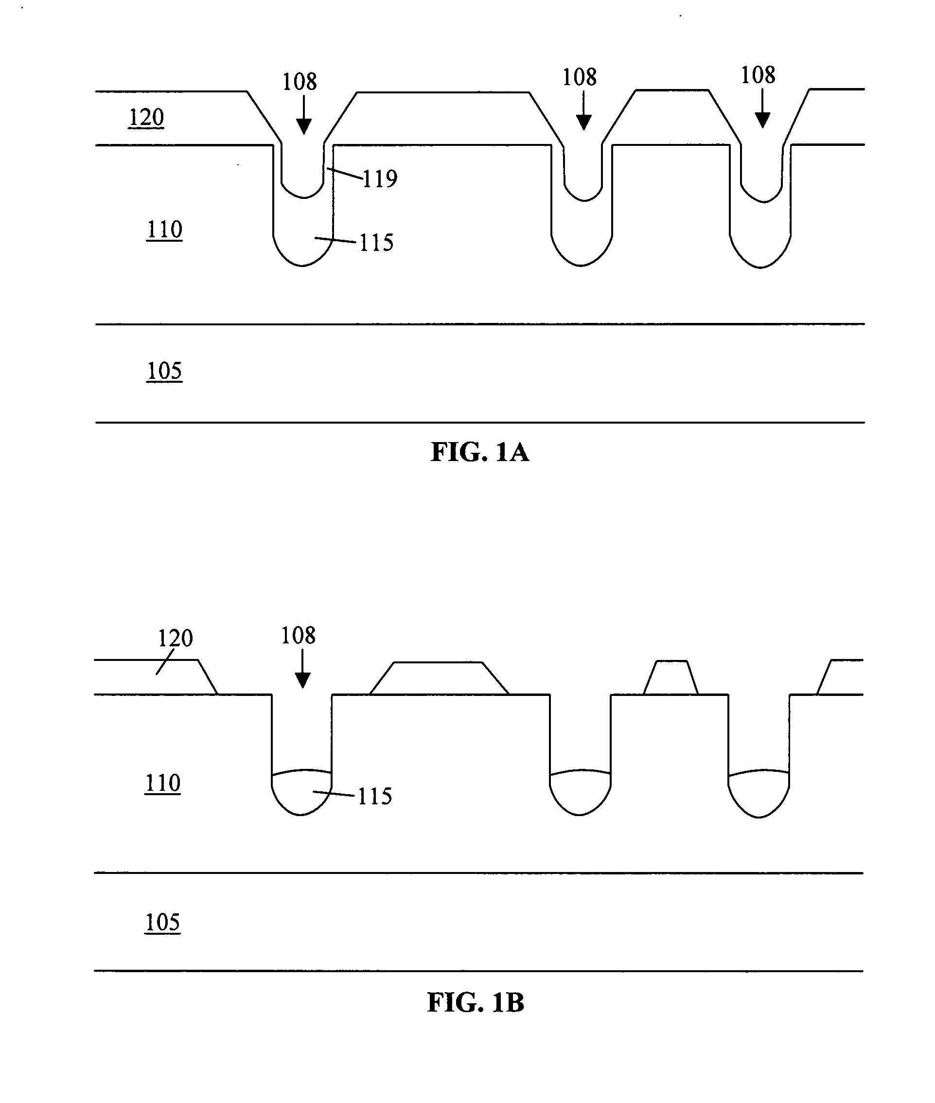
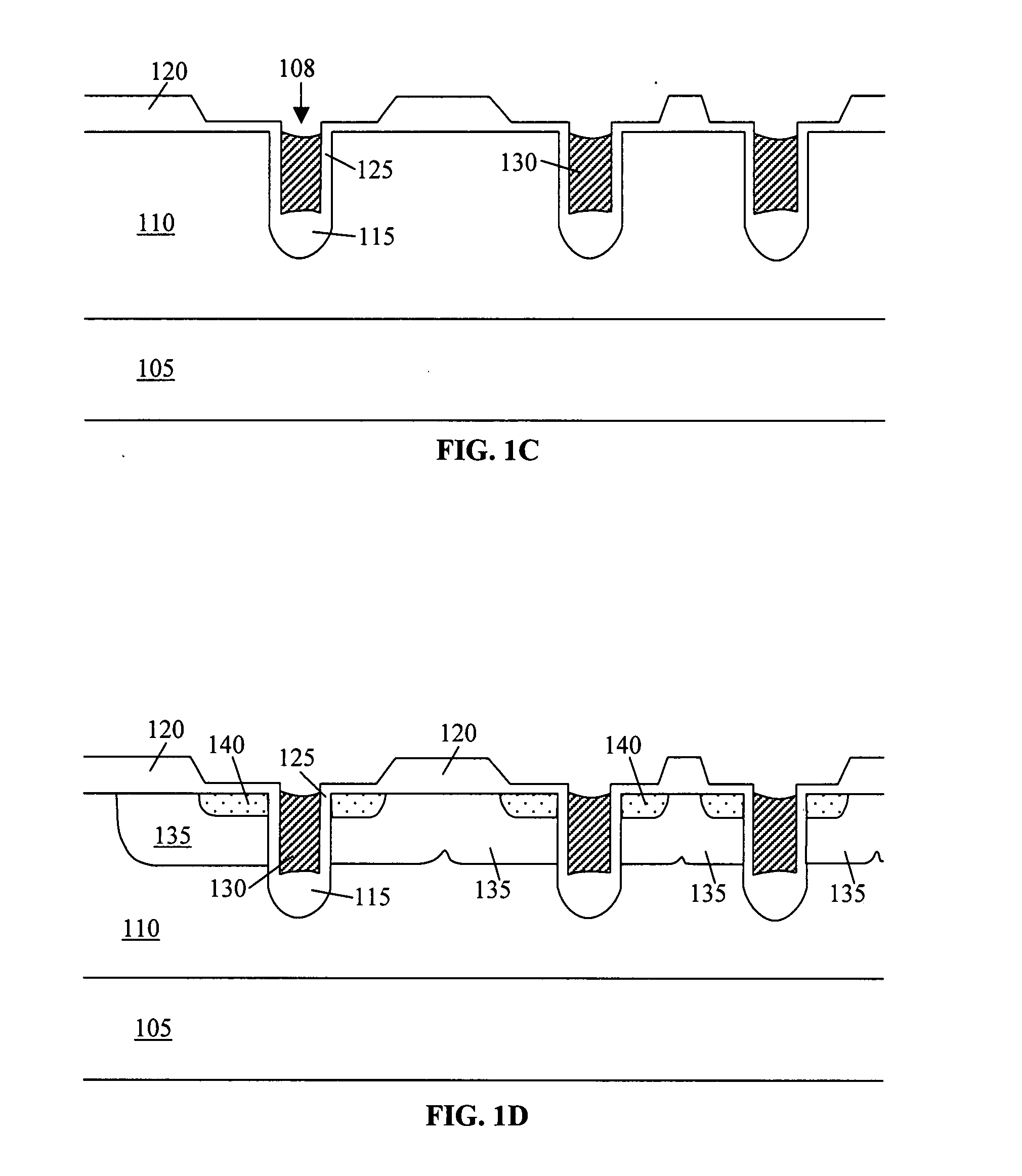
[0044]Referring to FIGS. 1A to 1G for a series of cross sectional views for describing the manufacturing processes of a new and improved trench MOSFET device of this invention. In FIG. 1A, a first mask (not shown) is first applied to open a plurality of trenches 108 into an epitaxial layer 110 supported on a semiconductor substrate 105. Then a high-density plasma (HDP) oxide layer is applied to form a thick oxide layer 115 at the trench bottom and thinner oxide layer 119 on trench sidewalls and thicker oxide layer 120 on the top surface of the substrate. In FIG. 1B, an oxide wet etch is carried out to etch out the thinner oxide layer 119 surrounding the sidewalls of the trench 108 and also a part of the thick oxide layer 120 near the trenches 108 and leaving only the thick oxide layer 120 in the mesa area and the thicker oxide layer 115 on the trench bottom. In FIG. 1C, a gate oxide layer 125 is then formed by thermal oxidation followed with filling the trenches 108 with polysilicon...


PUM


Abstract

This invention discloses a semiconductor power device. The trenched semiconductor power device includes a trenched gate, opened from a top surface of a semiconductor substrate, surrounded by a source region encompassed in a body region near the top surface above a drain region disposed on a bottom surface of a substrate. The semiconductor power device further includes an implanting-ion block disposed above the top surface on a mesa area next to the body region having a thickness substantially larger than 0.3 micron for blocking body implanting ions and source ions from entering into the substrate under the mesa area whereby masks for manufacturing the semiconductor power device can be reduced.

Description

BACKGROUND OF THE INVENTION[0001]1. Field of the Invention[0002]The invention relates generally to the semiconductor power devices. More particularly, this invention relates to an improved and novel manufacturing process and device configuration for providing the MOSFET device with trench gates having thick bottom trench oxide or split gate by applying high density plasma based manufacturing processes with reduced number of masks.[0003]2. Description of the Related Art[0004]In order to reduce the power consumptions and to increase the switching speed of a power semiconductor power device, it is desirable to further reduce the gate capacitance. Generally, in a trench gate MOSFET device, a reduced gate capacitance is achieved by forming a thick oxide layer on the trench bottom of the trench gate. Alternately, the trench gate is formed as a split gate to reduce the gate capacitance. However, in order to form a thick oxide layer on the trench bottom or a split gate with split and mutual...

Claims


Application Information

Patent Timeline
IPC IPC(8): H01L29/78H01L21/336H01L29/812H01L21/338
CPCH01L29/1095H01L29/407H01L29/42368H01L29/66734H01L29/7806H01L29/7811H01L29/7813
Inventor BHALLA, ANUPHEBERT, FRANCIOSTAI, SUNG-SHANLUI, SIK K.
Owner ALPHA & OMEGA SEMICON LTD
Why Eureka
Try Eureka