Thin-film aluminum nitride encapsulant for metallic structures on integrated circuits and method of forming same

a technology of aluminum nitride and metallic structure, which is applied in the direction of resistive material coating, superimposed coating process, liquid/solution decomposition chemical coating, etc., can solve the problems of degrading the accuracy of the sensor, changing the characteristics of the metal making up the structure, and reducing the vacuum environment

Inactive Publication Date: 2008-10-30
HEETRONIX
View PDF1 Cites 2 Cited by
  • Summary
  • Abstract
  • Description
  • Claims
  • Application Information

AI Technical Summary

Benefits of technology

[0009]ICs which employ a aluminum nitride (AlN) thin-film as an encapsulant are presented, in which the Al...

Problems solved by technology

Unfortunately, the metallic structures formed on an IC may be degraded by various mechanisms.
These high temperature steps can cause oxidation or act as a reducing or vacuum environment which may change the characteristics of the metal making up a structure.
For example, for a metallic environmental sensor as described above, exposure to an oxidizing atmosphere or a reducing or vacuum environment may alter ...

Method used


Image

  • Thin-film aluminum nitride encapsulant for metallic structures on integrated circuits and method of forming same
  • Thin-film aluminum nitride encapsulant for metallic structures on integrated circuits and method of forming same
  • Thin-film aluminum nitride encapsulant for metallic structures on integrated circuits and method of forming same

Examples


Embodiment Construction

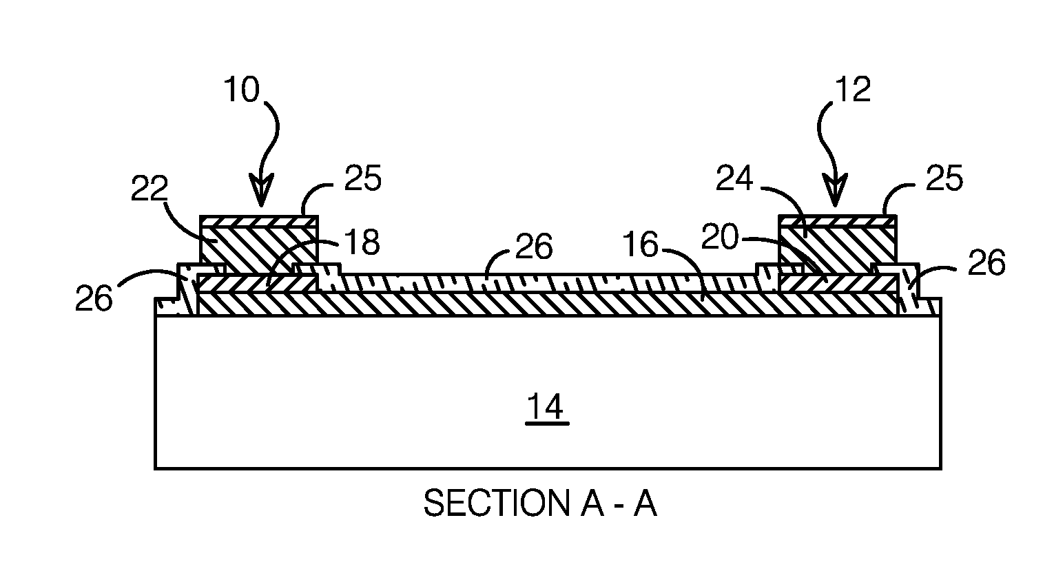
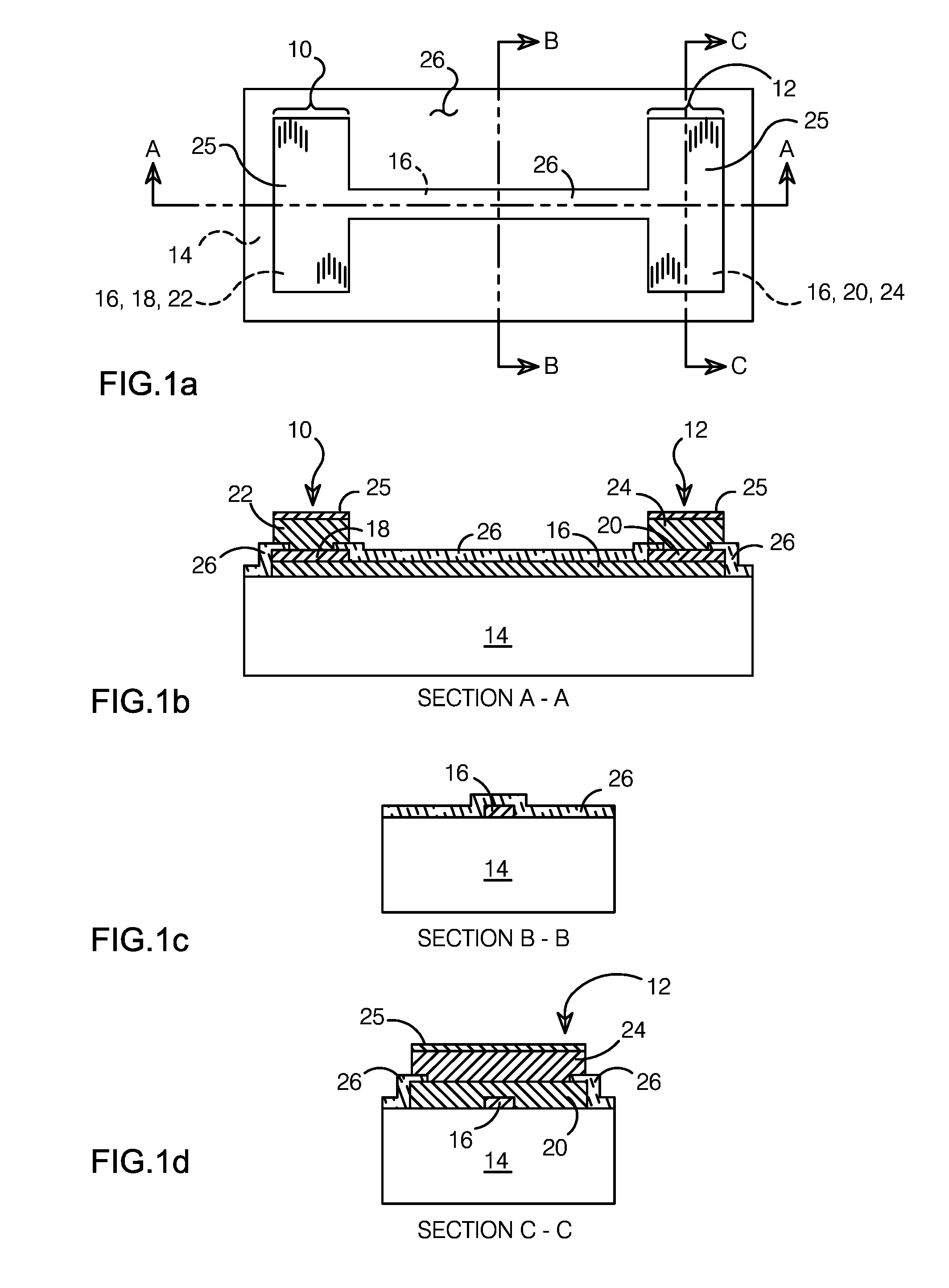
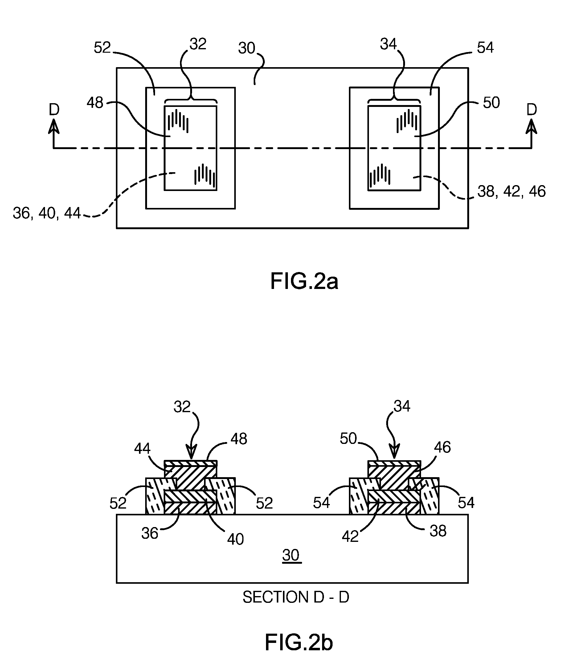
[0021]The present AlN thin-film encapsulant is advantageously employed over thin-film metallic circuitry such as an environmental sensor, on the vertical edges of an electrode pad, and / or over some or all of the surface area of an IC substrate. When used as described herein, the AlN thin-film acts to protect the encapsulated structures from exposure to an oxidizing atmosphere and from reducing and vacuum environments, electrically insulates them from other metallic structures, and may improve their adherence to the IC substrate's surface. Note, however, that to act as an effective encapsulant, the AlN thin-film must not chemically react with the conductive materials it is in contact with.

[0022]The principles of the invention are illustrated in the plan view of an IC shown in FIG. 1a, along with the cross-sectional views of the IC of FIG. 1a shown in FIGS. 1b, 1c and 1d, which are cut along section lines A-A, B-B and C-C, respectively. In this example, two metallic electrode pads 10,...


PUM

PropertyMeasurementUnit
Temperatureaaaaaaaaaa
Pressureaaaaaaaaaa
Structureaaaaaaaaaa

Abstract

An aluminum nitride (AlN) thin-film is applied over thin-film metallic circuitry such as an environmental sensor, on the side edges of electrode pads, and/or over some or all of the surface area of a substrate. The thin-film acts to protect the encapsulated structures from exposure to oxidation and from reducing and vacuum environments, electrically insulates the encapsulated structures from other structures, and helps to securely adhere the structures to the substrate surface. The AlN thin-film can also enable multiple IC layers to be stacked on top of each other, with AlN thin-film interlayers employed between IC layers such that each IC layer is separated and electrically insulated from adjacent layers.

Description

RELATED APPLICATIONS[0001]This application claims the benefit of provisional patent application No. 60 / 926,677 to James D. Parsons and Gregg B. Kruaval, filed Apr. 26, 2007.BACKGROUND OF THE INVENTION[0002]1. Field of the Invention[0003]This invention relates generally to integrated circuits (ICs), and more particularly to means of encapsulating metallic structures formed on an IC substrate.[0004]2. Description of the Related Art[0005]Integrated circuits comprise a semiconductor substrate upon which are formed various structures which are interconnected to form a circuit. Signals are conveyed to and from the chip via input / output (I / O) electrode pads which connect to the on-chip circuitry; lead wires are typically soldered or welded to the electrode pads to carry the signals to and from the chip.[0006]Some IC structures are metallic. For example, the metallization that interconnects on-chip circuits with each other and with the electrode pads, as well as the electrode pads themselve...

Claims


Application Information

Patent Timeline
IPC IPC(8): H01L23/29H05K3/00H01L21/56
CPCH01L23/291H01L2924/0002H01L2924/00
Inventor PARSONS, JAMES D.KRUAVAL, GREGG B.
Owner HEETRONIX
Why Eureka
Try Eureka