Method of microwave annealing for enhancing organic electronic devices
- Summary
- Abstract
- Description
- Claims
- Application Information
AI Technical Summary
Benefits of technology
Problems solved by technology
Method used
Image


Examples
Embodiment Construction
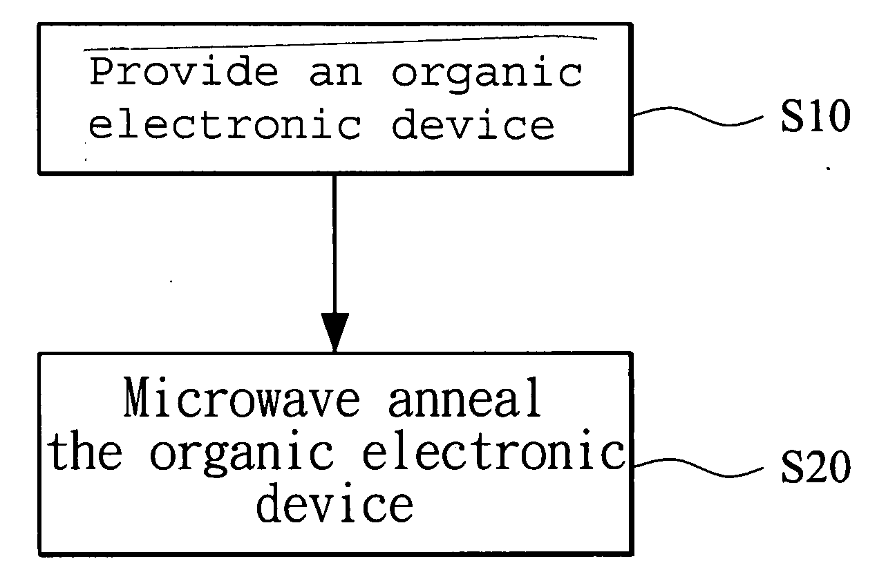
[0038]As shown in FIG. 1, a method of microwave annealing for enhancing the properties of an organic electronic device 20 is disclosed, comprising: providing an organic electronic device S10; and microwave annealing the organic electronic device S20.
[0039]Provide an organic electronic device S10; the organic electronic device 20 may be an organic solar cell, an organic light detector, an organic light emitting diode, or an organic thin film transistor.
[0040]As shown in FIG. 2A, the organic electronic device 20 comprises a substrate 21 having a first conductive layer 22 formed thereon, the organic electronic device 20 is fabricated from forming an organic active layer 23 on the substrate 21, and then forming a second conductive layer 24 on the organic active layer 23, so that the organic electronic device 20 is formed as a sandwich structure in which the order of layers is “the first conductive layer 22—the organic active layer 23—the second conductive layer 24” from the bottom up.
[0...
PUM
| Property | Measurement | Unit |
|---|---|---|
| Time | aaaaa | aaaaa |
| Time | aaaaa | aaaaa |
| Time | aaaaa | aaaaa |
Abstract
Description
Claims
Application Information