Electromagnetic Wave Shielding Sheet and Process For Producing the Same

Inactive Publication Date: 2008-11-13
DAI NIPPON PRINTING CO LTD
View PDF12 Cites 27 Cited by
  • Summary
  • Abstract
  • Description
  • Claims
  • Application Information

AI Technical Summary

Benefits of technology

[0020]The present invention provides an electromagnetic wave shielding sheet having moderate transparency and high electromagnetic wave shielding ability, comprising mesh line parts that do not reflect extraneous light to make the mesh highly invisible, to make image contrast high in the presence of extraneous light, and to make a displayed image highly visible. Further, if a specific material is selected to form the blackening layer, the formation of the blackening layer only on one surface of the metal layer is sufficient to fulfill the purpose. Falling off the blackening layer and an increase in material cost are th

Problems solved by technology

However, such a metal mesh layer is disadvantageous in that, since it is highly lustrous and reflects extraneous light such as sunlight, the mesh is noticeable, and, moreover, a screen appears white due to the metal mesh layer to decrease image contrast.
However, so far as this means is employed, it is impossible to blacken the transparent-substrate-side surface of the metal layer.
Therefore, this means cannot cope with such a design that an electromagnetic wave shielding sheet is mounted on a display with the transparent substrate side of the sheet facing to the observer side.
In addition, it takes a long time for plating if electrically conductive ink is used because such ink has high electrical resistance.
In this pr

Method used


Image

  • Electromagnetic Wave Shielding Sheet and Process For Producing the Same
  • Electromagnetic Wave Shielding Sheet and Process For Producing the Same
  • Electromagnetic Wave Shielding Sheet and Process For Producing the Same

Examples


example 1

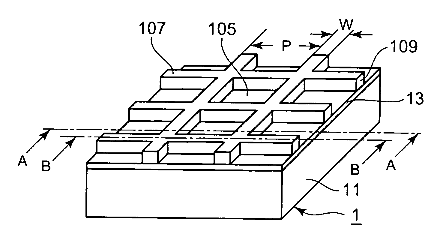
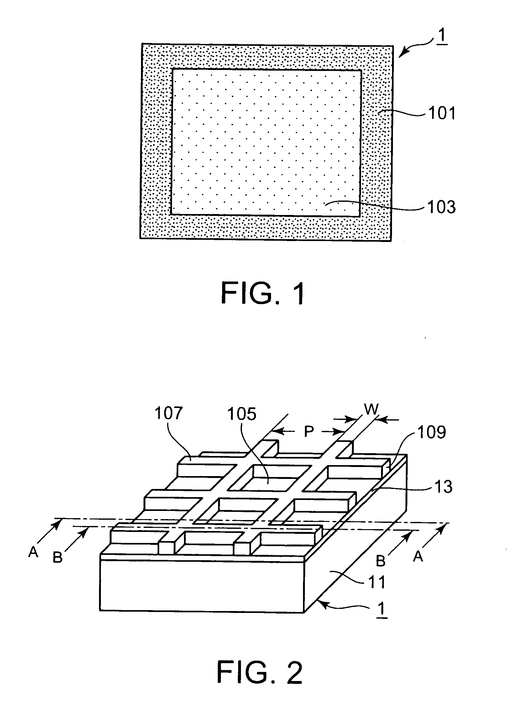
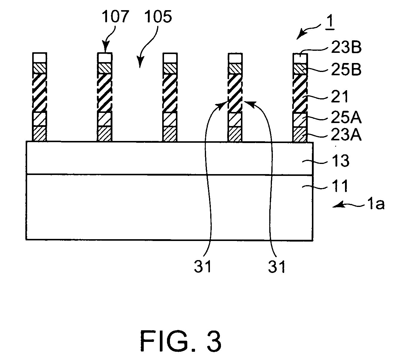
[0086]Electrolytic copper foil with a thickness of 10 μm was used as the metal layer 21. Copper-cobalt alloy particles (mean particle diameter: 0.3 μm) were cathodically electrodeposited on one surface of the metal layer 21, thereby conducting blackening treatment to form a blackening layer 25A. After plating the metal layer 21 with zinc, conventional chromate treatment was conducted by a dipping method to form anticorrosive layers containing zinc and chromium on both surfaces of the metal layer 21. The anticorrosive layer present on the surface of the blackening layer 25A is herein referred to as an anticorrosive layer 23A, and the anticorrosive layer present on the surface of the metal layer 21 is referred to as a second anticorrosive layer 23B.

[0087]The surface of the metal layer 21 on the anticorrosive layer 23A and a transparent substrate 11 made of a PET film A4300 (trademark of a polyethylene terephthalate film, manufactured by Toyobo Co., Ltd., Japan) with a thickness of 100...

example 2

[0091]An electromagnetic wave shielding sheet 1 was obtained in the same manner as in Example 1, provided that blackening treatment is conducted by cathodically electrodepositing copper-cobalt alloy particles (mean particle diameter: 0.3 μm) on both surfaces of electrolytic copper foil with a thickness of 10 μm, serving as the metal layer 21.


PUM

PropertyMeasurementUnit
Currentaaaaaaaaaa
Currentaaaaaaaaaa
Transparencyaaaaaaaaaa

Abstract

An electromagnetic wave shielding sheet 1 comprises a transparent substrate 11, and line parts 107 that define openings 105, provided on the transparent substrate 11. The line parts 107 have a metal mesh layer 21, and a blackening layer 25A formed on the surface of the metal layer 21, on the side of the transparent substrate 11. Matted layers 31 are formed on the side faces of the line parts 107, and an anticorrosive layer 23A is provided between the blackening layer 25A and the transparent substrate 11.

Description

FIELD OF THE INVENTION[0001]The present invention relates to an electromagnetic wave shielding sheet for preventing EMI (electromagnetic interference) that is caused by such displays as cathode ray tubes (hereinafter also referred to as CRTs) and plasma display panels (hereinafter also referred to as PDPs), and, more particularly, to an electromagnetic wave shielding sheet that makes a displayed image highly visible and that can be produced in a small number of steps, and to a process for producing the electromagnetic wave shielding sheet.[0002]In this Specification, “ratio”, “part”, “%”, and the like that indicate proportions are on a weight basis unless otherwise specified, and the symbol “ / ” denotes that layers enumerated together with this symbol are integrally laminated. Further, “NIR” and “PET” designate “near infrared rays” and “polyethylene terephthalate”, respectively, and are abbreviations, synonyms, functional expressions, common designations, or terms used in the art.BAC...

Claims


Application Information

Patent Timeline
IPC IPC(8): H05K9/00H05K3/00B32B15/08C23C22/24C25D7/06C25D11/38G09F9/00
CPCC25D15/02H01F41/34Y10T29/49124H05K9/0096H01J2211/446H05K9/00
Inventor NAITO, NOBUOARAKAWA, FUMIHIROMASAKI, TADAHIRO
Owner DAI NIPPON PRINTING CO LTD
Why Eureka
Try Eureka