Small pixel for image sensors with JFET and vertically integrated reset diode

a technology of image sensor and reset diode, which is applied in the direction of electrical equipment, semiconductor devices, radio frequency control devices, etc., can solve the problems of circuit sharing, ktc-reset noise generation, and low cost of cmos image sensor, and achieve low noise performan

Active Publication Date: 2008-11-20
INTELLECTUAL VENTURES II
View PDF7 Cites 18 Cited by
  • Summary
  • Abstract
  • Description
  • Claims
  • Application Information

AI Technical Summary

Benefits of technology

[0008]Embodiments of the present invention are directed to providing a pixel and a pixel array of an image sensor device with small pixel sizes by resetting sensed charge using a diode built vertically above a substrate. It also provides a pixel and a pixel array of an image sensor device with low noise performance by using a JFET as a source follower transistor for sensing charge.

Problems solved by technology

This step removes charge collected on the FD node; however, it generates kTC-reset noise as is well known in the art.
However, the three transistors still occupy a significant amount of the valuable active pixel area, which is a problem for further reduction of pixel size and thus for lowering the cost of the CMOS image sensors.
This disadvantage is often times compensated by sharing the pixel circuit with several photo diodes.
However, the circuit sharing has also its disadvantages.
Other disadvantages of the sharing concept are slightly asymmetrical layout and electrical functions that result is some asymmetrical optical as well as electrical cross talk problems.

Method used


Image

  • Small pixel for image sensors with JFET and vertically integrated reset diode
  • Small pixel for image sensors with JFET and vertically integrated reset diode
  • Small pixel for image sensors with JFET and vertically integrated reset diode

Examples


Embodiment Construction

[0020]Hereinafter, exemplary embodiments of the present invention will be described in detail with reference to accompanying drawings.

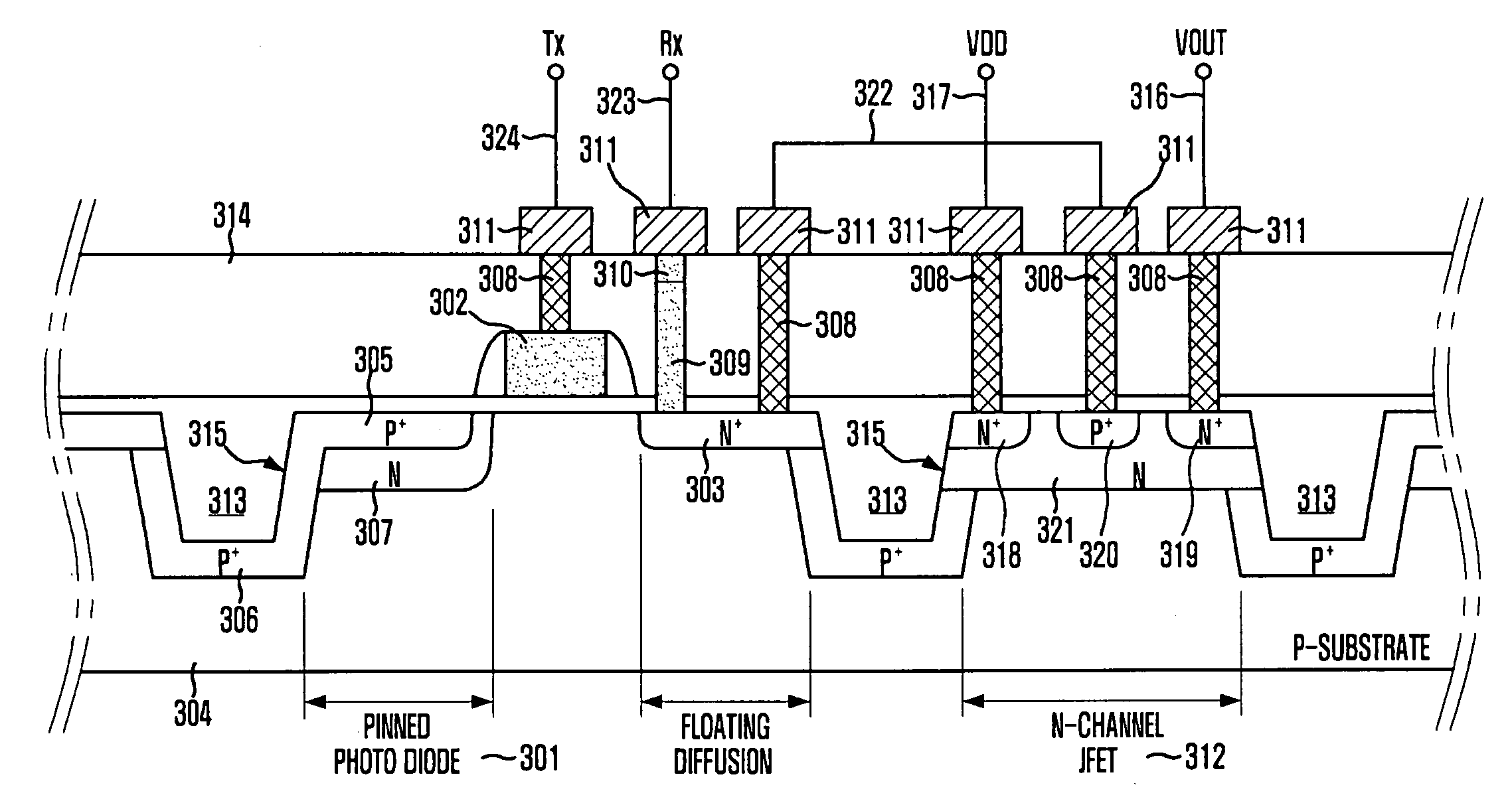
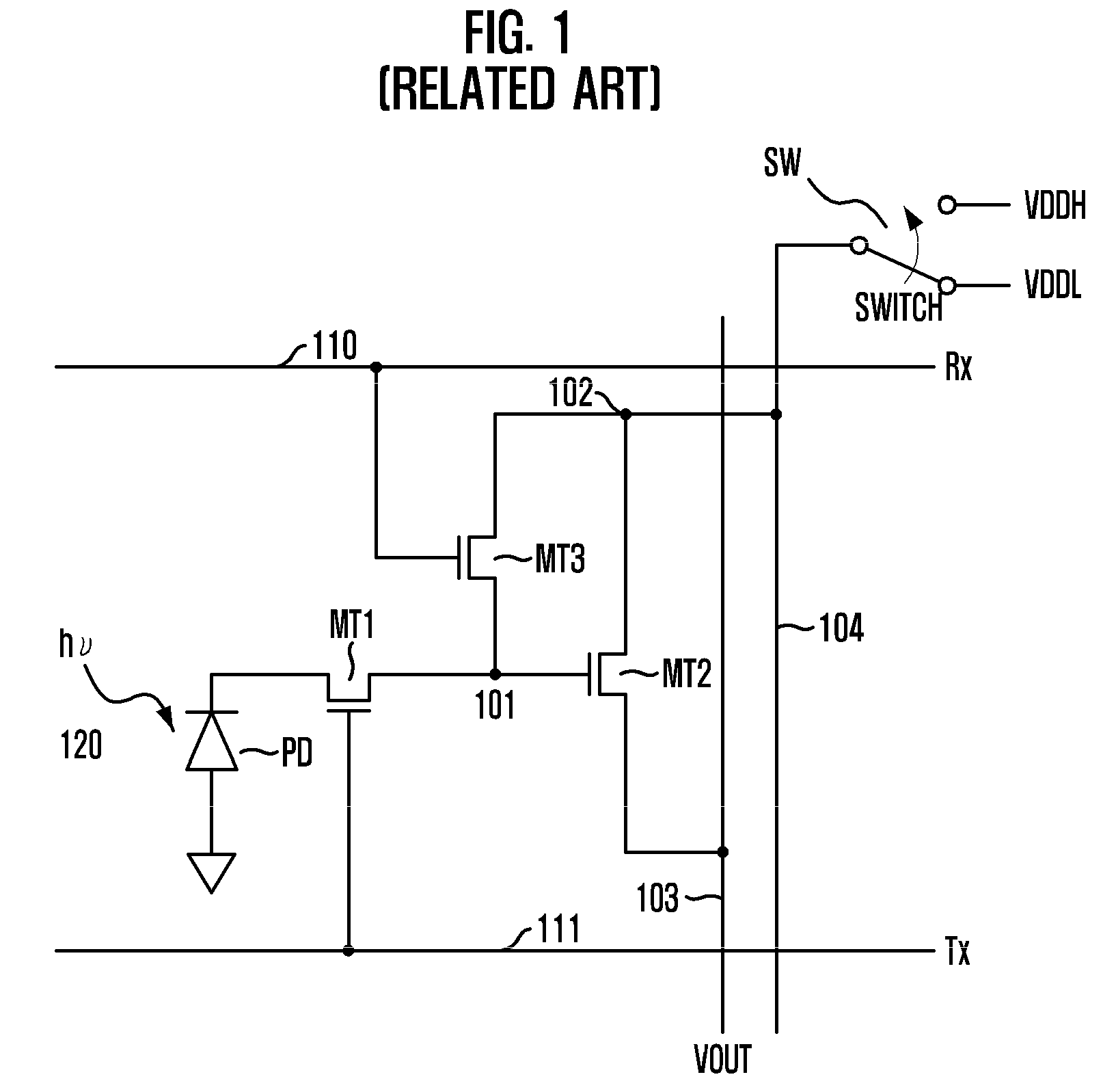
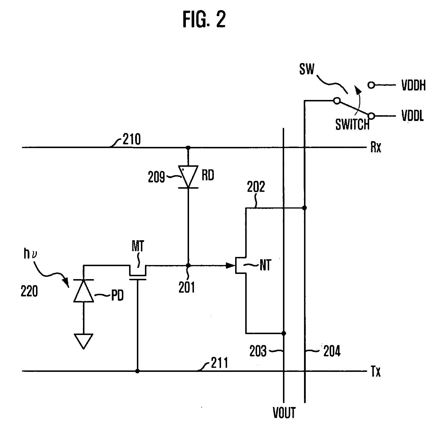
[0021]FIG. 2 is a schematic circuit diagram of a pixel in accordance of present invention. The pixel includes a pinned photodiode PD, a MOS transistor MT, an n-channel JFET NT and a p-n diode RD. The pinned photodiode PD is coupled through the MOS transistor MT, i.e., a charge transfer transistor, to a charge detection floating diffusion (FD) node 201. The FD node 201 is reset by the p-n diode RD that is connected to a reset line 210. The voltage on the FD node 201 is sensed by the n-channel JFET NT, i.e., a source follower transistor. The n-channel JFET NT has its gate connected to FD node 201, the source connected to an output column bus line 203, and the drain connected to a drain bus line 204 through a drain node 202. The drain bus line 204 is connected to a drain switch SW that has a capability to switch the drain voltage between two levels VDDH ...


PUM


Abstract

A pixel and a pixel array of an image sensor device of the present invention have small pixel sizes by resetting sensed charge using a diode built vertically above a substrate. The pixel and the pixel array also have low noise performance by using a JFET as a source follower transistor for sensing charge. The pixel includes a floating diffusion node configured to sense photo-generated charge, a reset diode configured to reset the floating diffusion node in response to a reset signal, and a junction field effect transistor configured to output a signal having an output voltage level corresponding to a charge level of the floating diffusion node.

Description

CROSS-REFERENCE(S) TO RELATED APPLICATIONS[0001]The present invention claims priority to Korean patent application number 10-2007-0046617, filed on May 14, 2007, which is incorporated by reference in its entirety.BACKGROUND OF THE INVENTION[0002]The present invention relates to solid-state image sensors, specifically to Complementary Metal-Oxide-Semiconductor (CMOS) image sensors that have very small pixel sizes. In more particular the present invention relates to pixels that use only two transistors (2T) and a diode for the reset and addressing instead of the typical reset and addressing transistors. Further more the diode can be built vertically on top of the silicon substrate and have a very small size in order not to occupy the valuable pixel area. A Source Follower (SF) MOS transistor for sensing charge has been replaced in this pixel by a depletion mode n-channel Junction gate Field-Effect Transistor (JFET), which gives the pixel very low noise performance. The described pixel...

Claims


Application Information

Patent Timeline
Patent Type & Authority Applications(United States)
IPC IPC(8): H01L31/00
CPCH01L27/14603H01L27/1463H01L27/14609H01L27/146
Inventor HYNECEK, JAROSLAV
Owner INTELLECTUAL VENTURES II
Why Eureka
Try Eureka