Semiconductor device and manufacturing method thereof

a technology of semiconductor devices and semiconductors, applied in semiconductor devices, basic electric elements, electrical equipment, etc., can solve the problems of increasing manufacturing costs suppress the short-channel effect, suppress the variation in electrical characteristics of the second transistor

Inactive Publication Date: 2008-11-20
PANASONIC CORP
View PDF11 Cites 18 Cited by
  • Summary
  • Abstract
  • Description
  • Claims
  • Application Information

AI Technical Summary

Benefits of technology

[0018]Thereby, in the second transistor, the ratio of the amount of the first conductivity type impurity in the second pocket region to the amount of a first conductivity type impurity introduced for adjustment of the threshold voltage can be reduced, so that a variation in electrical characteristics of the second transistor can be suppressed while suppressing a short-channel effect in the first transistor. This is particularly effective when the first transistor and the second transistor have the same power supply voltage and when the second transistor has a gate length longer than that of the first transistor.
[0019]In a method for manufacturing the semiconductor device of the present invention, at least a source-side pocket region of the second pocket regions in the second transistor is formed at the same time when pocket regions of a third transistor are formed. Thereby, the semiconductor device in which a variation in electrical characteristics of the second transistor can be suppressed while suppressing a short-channel effect in the first transistor, can be manufactured by a smaller number of steps.

Problems solved by technology

However, in the technique of Japanese Unexamined Patent Application Publication No. 2003-509863, a mask for preventing a pocket region from being formed in the active region of an analog transistor is additionally formed, resulting in an increase in manufacturing cost.

Method used


Image

  • Semiconductor device and manufacturing method thereof
  • Semiconductor device and manufacturing method thereof
  • Semiconductor device and manufacturing method thereof

Examples


first embodiment

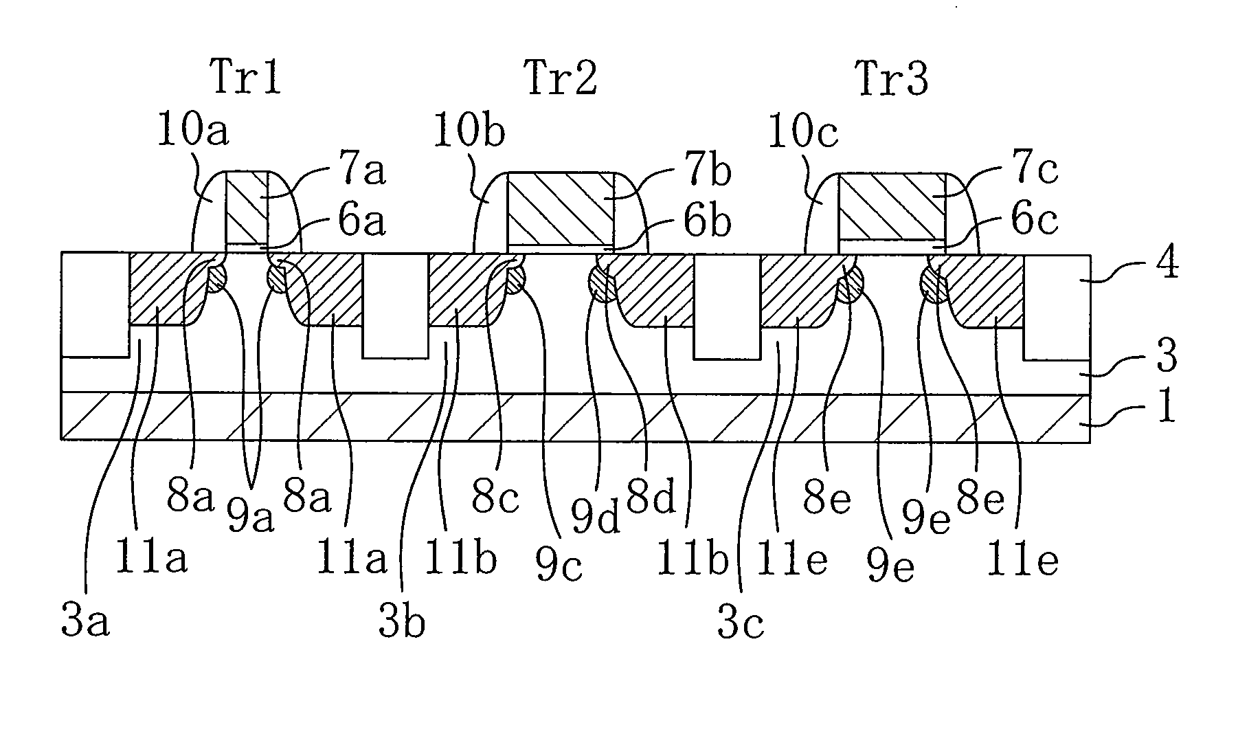
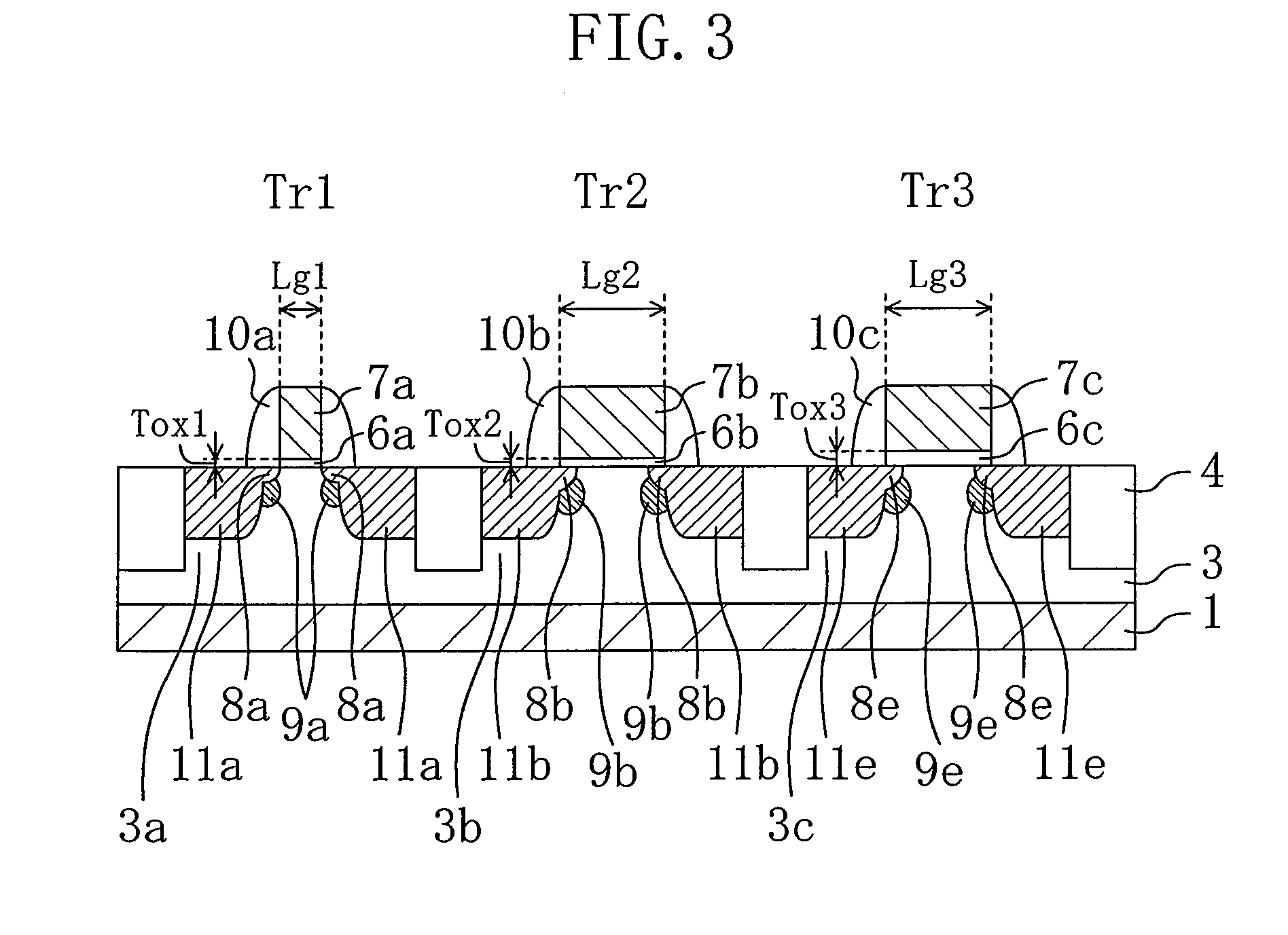
[0038]FIG. 3 is a cross-sectional view showing a semiconductor device according to a first embodiment of the present invention. In this embodiment, an N-channel MOS transistor will be described as an example, though the present invention is also applicable to a P-channel MOS transistor. In FIG. 3, Tr1 indicates a 1.2-V core transistor, Tr2 indicates a 1.2-V analog transistor, and Tr3 indicates a 1.8-V transistor. Although Tr3 is assumed to be a 1.8-V transistor in this embodiment, a 2.5- or 3.3-V transistor can also be applicable to the semiconductor device of the present invention. Note that an “analog transistor” refers to a transistor which executes an analog function in a circuit. Although most analog transistors have a longer gate length than that of core transistors, an analog transistor may have basically the same structure as that of a core transistor.

[0039]As shown in FIG. 3, the semiconductor device of this embodiment comprises a P-type well 3 provided in a P-type semicond...

second embodiment

[0054]FIG. 5 is a cross-sectional view showing a semiconductor device according to a second embodiment of the present invention. In this embodiment, an N-channel MOS transistor will be described as an example, though the present invention is also applicable to a P-channel MOS transistor. In FIG. 5, Tr1 indicates a 1.2-V core transistor, Tr2 indicates a 1.2-V analog transistor, and Tr3 indicates a 1.8-V transistor. Although Tr3 is assumed to be a 1.8-V transistor in this embodiment, a 2.5- or 3.3-V transistor can also be applicable to the semiconductor device of the present invention. Note that, in FIG. 5, the same parts as those of the semiconductor device of the first embodiment of FIG. 3 are indicated by the same reference symbols. In the semiconductor device of this embodiment, the transistors Tr1 and Tr3 have the same structures as those of the semiconductor device of the first embodiment.

[0055]As shown in FIG. 5, the semiconductor device of this embodiment is characterized in t...


PUM


Abstract

A semiconductor device includes a first conductivity type well formed on a semiconductor substrate, and a first transistor and a second transistor formed on the well. The first transistor has first pocket regions containing a first conductivity type impurity and first source/drain regions containing a second conductivity type impurity, and the second transistor has second pocket regions containing a first conductivity type impurity and second source/drain regions containing a second conductivity type impurity, and executes an analog function. A concentration of the first conductivity type impurity contained in the source-side and the drain-side second pocket regions is lower than a concentration of the first conductivity type impurity included in the first pocket regions.

Description

BACKGROUND OF THE INVENTION[0001]1. Field of the Invention[0002]The present invention relates to a semiconductor device and a manufacturing method thereof. More particularly, the present invention relates to a semiconductor device structure having a less variation in characteristics and an implanting method for producing the same.[0003]2. Description of the Related Art[0004]As the miniaturization advances, the cell area of an SRAM (Static Random Access Memory) is reduced in accordance with scaling. A power supply voltage applied to an SRAM cell is currently as low as about 1.2 V. A sense amplifier, for which a considerably small variation in characteristics is required, includes a 1.2-V transistor as in the SRAM cell, but the gate length of the transistor is not minimum, and is relatively large, specifically about four times as large as the minimum gate length. Therefore, the sense amplifier, which requires a large drive force, is also designed to have a large gate width. To reduce ...

Claims


Application Information

Patent Timeline
Patent Type & Authority Applications(United States)
IPC IPC(8): H01L29/00H01L21/336
CPCH01L21/823412H01L21/823456H01L21/823462H01L29/1083
Inventor YAMASHITA, KYOJIIKOMA, DAISAKU
Owner PANASONIC CORP
Why Eureka
Try Eureka