Negative Feedback Avalanche Diode

a diode and negative feedback technology, applied in the field of single-photon avalanche photodetectors, can solve the problem that the diode cannot be operable for photons having wavelengths, and achieve the effect of increasing the capacitance of the photodetector structur

Active Publication Date: 2008-11-20
LG INNOTEK CO LTD
View PDF4 Cites 14 Cited by
  • Summary
  • Abstract
  • Description
  • Claims
  • Application Information

AI Technical Summary

Benefits of technology

[0021]In contrast to the prior art, the present invention employs passive quenching within a single-photon photodetector that IS operable at wavelengths longer than 900 nm. Since the MRS structure is not easily fabricated using III-V or II-VI semiconductor material systems, however, passive quenching has been accomplished in the present invention by means of a thin-film resistor that is mo...

Problems solved by technology

These MRS Photodiodes are not operable for photon...

Method used


Image

  • Negative Feedback Avalanche Diode
  • Negative Feedback Avalanche Diode
  • Negative Feedback Avalanche Diode

Examples


Embodiment Construction

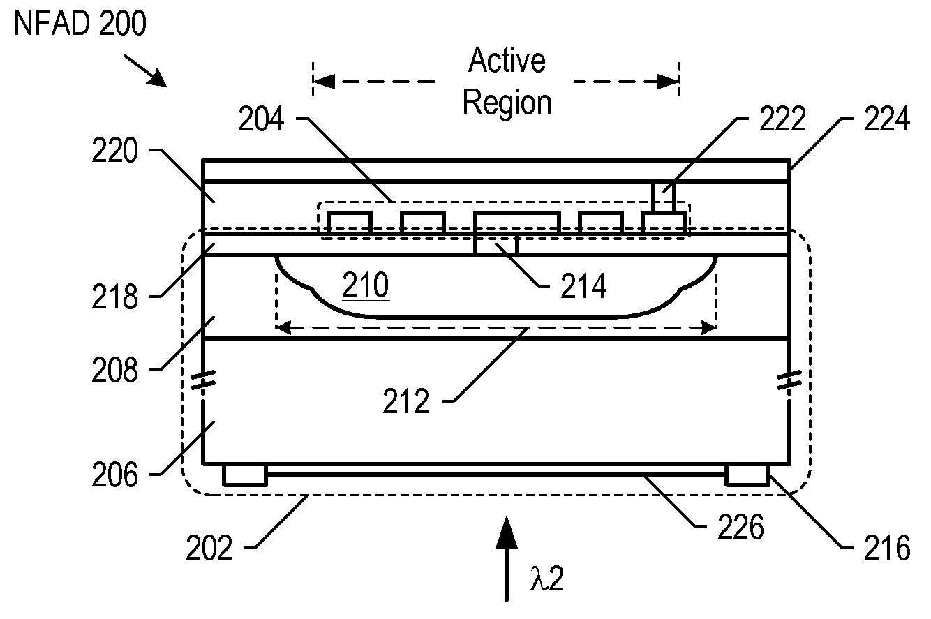
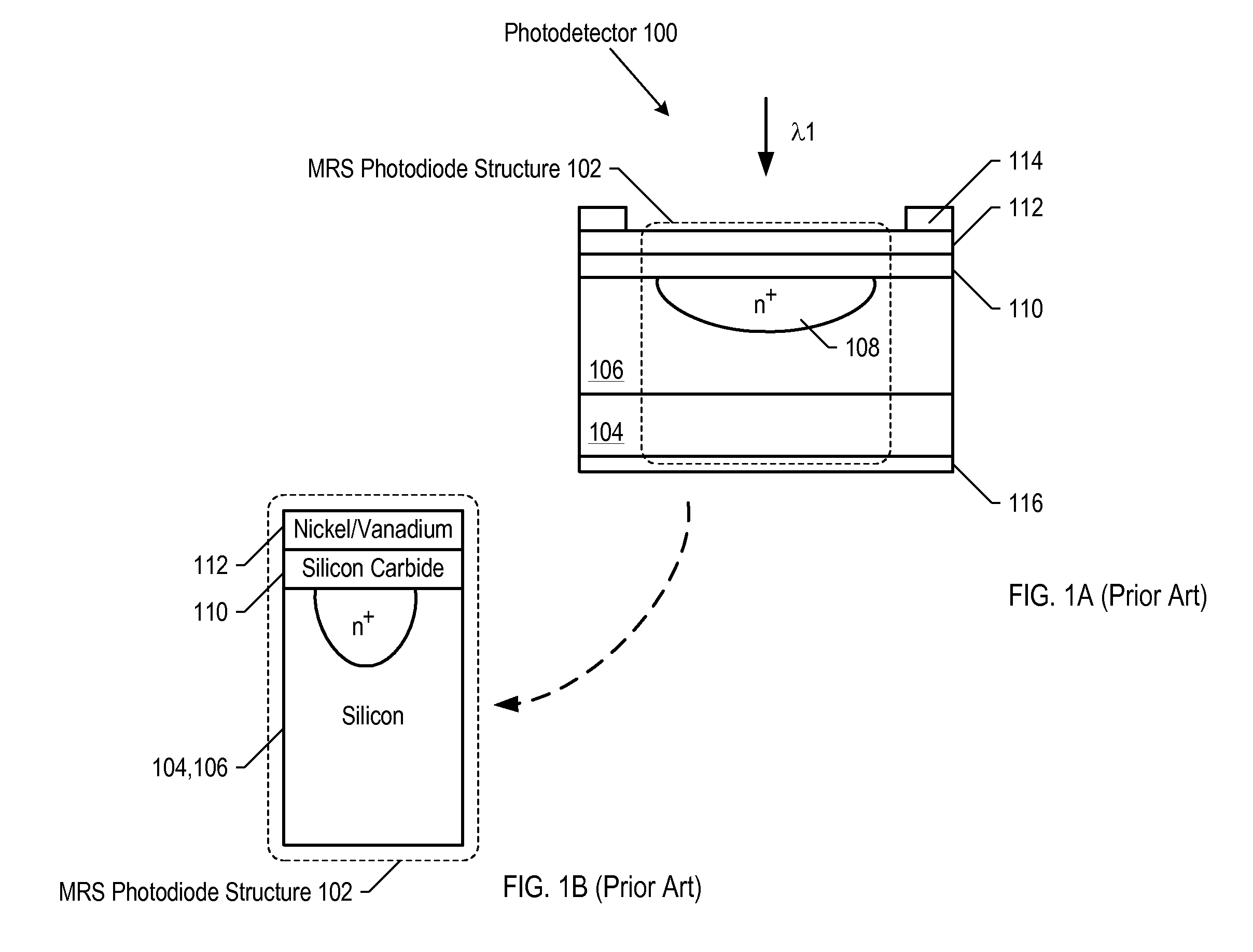
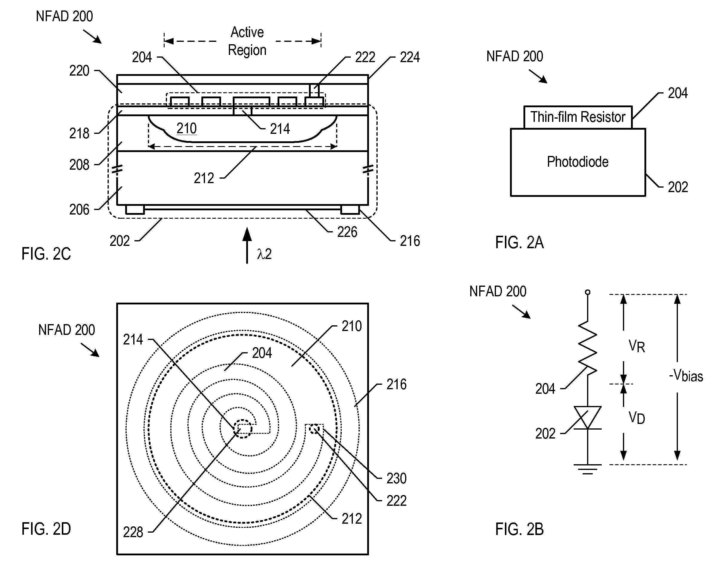
[0033]The following terms are defined for use in this Specification, including the appended claims:[0034]Electrically-coupled means that two elements are in either direct or indirect electrical communication. This can be via direct physical contact (e.g., a plug in an electrical outlet, etc.), via an electrically-conductive intermediate (e.g., a wire or conductive trace that interconnects the devices, etc.), or via one or more intermediate devices, etc. (e.g., resistors, capacitors, transistors, etc.).[0035]Electrically-connected means that two elements are in direct electrical contact without any intervening devices (e.g., resistors, capacitors, transistors, etc.). In other words, the point or region of contact between the two elements remains at a substantially uniform voltage for substantially any current (i.e., the two elements are “shorted” together). For the purposes of this definition, an electrically-conductive wire or trace that serves only to interconnect the two elements ...


PUM


Abstract

A single-photon avalanche detector is disclosed that is operable at wavelengths greater than 1000 nm and at operating speeds greater than 10 MHz. The single-photon avalanche detector comprises a thin-film resistor and avalanche photodiode that are monolithically integrated such that little or no additional capacitance is associated with the addition of the resistor.

Description

FIELD OF THE INVENTION[0001]The present invention relates to avalanche photodetectors in general, and, more particularly, to single-photon avalanche photodetectors.BACKGROUND OF THE INVENTION[0002]Photodetectors capable of detecting a single-photon (a single “particle” of optical energy) are useful in many applications. To date, most of these applications have relied on the use of single-photon detectors such as photomultiplier tubes (PMTs) or single-photon avalanche detectors (SPADs) that are silicon-based, and are therefore capable of efficiently detecting only photons that have a wavelength within the range of approximately 250 nanometers (nm) to approximately 900 nm. New applications are emerging, however, that require single-photon detectors that can operate at high speed (>1 MHz) and at longer wavelengths (>1000 nm). Such devices would find use in areas such as: quantum information processing, quantum computing, quantum cryptography, and quantum teleportation and communi...

Claims


Application Information

Patent Timeline
IPC IPC(8): H01L31/107H01L31/18
CPCH01L31/02027H01L31/1032H01L31/1035H01L31/107
Inventor ITZLER, MARK ALLEN
Owner LG INNOTEK CO LTD
Why Eureka
Try Eureka