Organic light emitting diode and flat panel device including the same

a light-emitting diode and organic technology, applied in the direction of luminescent compositions, natural mineral layered products, chemistry apparatus and processes, etc., can solve the problems of reducing the lifetime of the organic light-emitting diode, and achieve the effect of high charge transporting ability and electric stability

Inactive Publication Date: 2008-11-20
SAMSUNG MOBILE DISPLAY CO LTD
View PDF12 Cites 10 Cited by
  • Summary
  • Abstract
  • Description
  • Claims
  • Application Information

AI Technical Summary

Benefits of technology

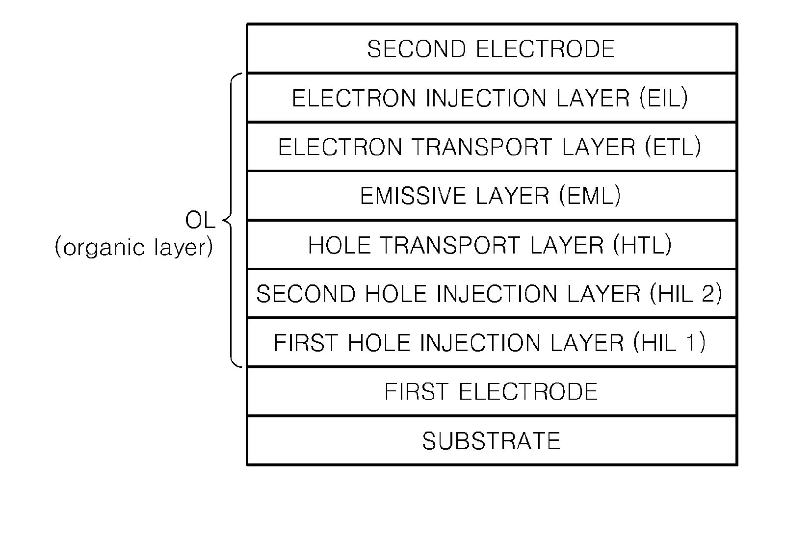
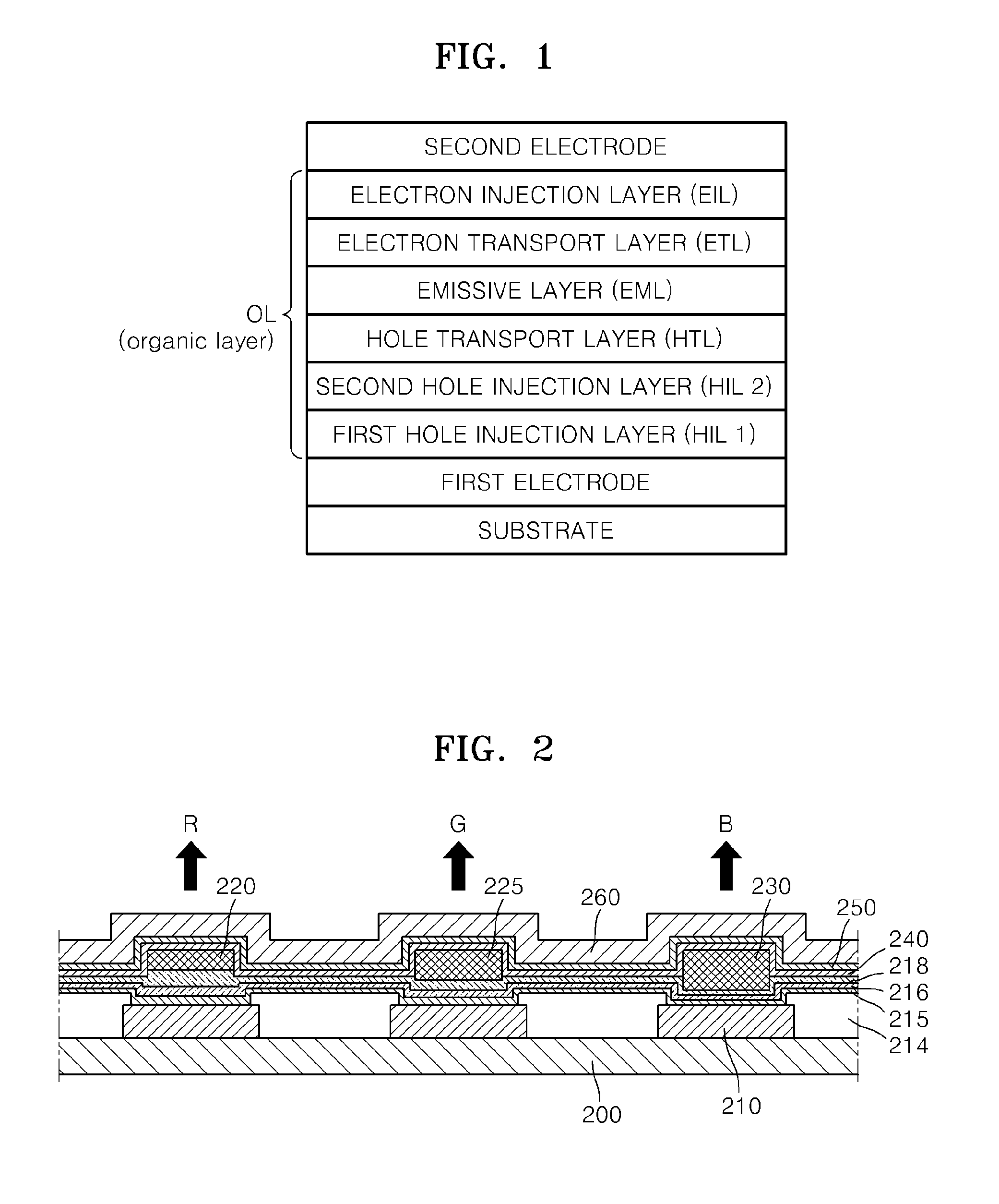
[0008]Aspects of the present invention provide an organic light emitting diode including an organic layer disposed between a pair of electrodes, and the organic layer comprises a compound containing at least one fluorine group that can trap electrons, thereby having electrical stability and high charge transporting ability, and a flat display device including the organic light emitting diode.
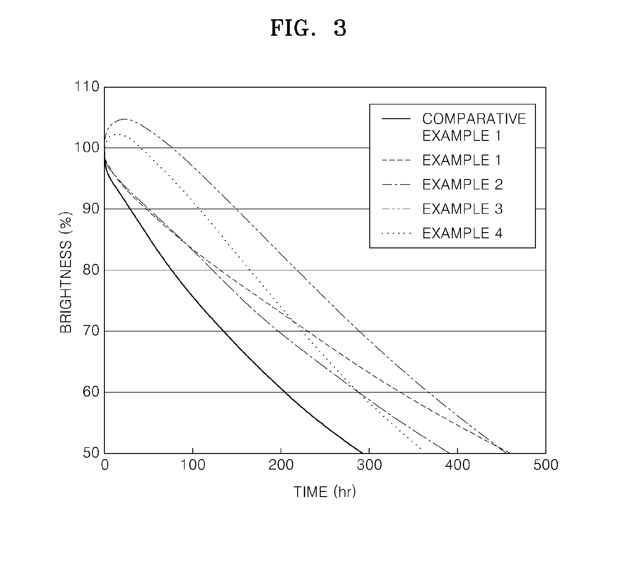
[0012]The organic light emitting diode according to aspects of the present invention can have long life-time.

Problems solved by technology

Such collisions lead to a decreased lifetime of the organic light emitting diode, and thus, an organic material forming an organic layer that can trap electrons is required.

Method used


Image

  • Organic light emitting diode and flat panel device including the same
  • Organic light emitting diode and flat panel device including the same
  • Organic light emitting diode and flat panel device including the same

Examples


synthesis example 1

Compound 3 (Preparation of 4,4′-bis[(N-(3-(9-phenyl-9H)carbazolyl)-N-(4-fluorophenyl)amino]biphenyl

[0088]Compound 3 was synthesized according to Reaction Scheme 2 below.

Synthesis of Intermediate A (9-phenyl-9H-carbazole)

[0089]16.7 g of carbazole (100 mmol), 26.5 g of iodobenzene (130 mmol), 1.9 g of CuI (10 mmol), 138 g of K2CO3 (1 mol), and 530 mg of 18-crown-6 (2 mmol) were dissolved in 500 ml of 1,3-Dimethyl-3,4,5,6-tetrahydro-(1H)-pyrimidinone (DMPU), and then heated at 170° C. for 8 hours. After the reaction was terminated, a reaction mixture was cooled to room temperature, and then a resulting solid material was filtered. Then, a small amount of ammonia water was added to the filtered water and washed three times using 300 ml of diethylether. The obtained diethylether layer was dried using anhydrous MgSO4 and then dried under low pressure to obtain a product. The product was purified with silicagel column chromatography to obtain 22 g (yield: 90%) of white solid Intermediate A...

synthesis example 2

Preparation of Compound II (4,4′-bis[(N-(3-(9-(4-fluorophenyl)-9H)carbazolyl)-N-phenylamino]biphenyl)

[0095]Compound II was synthesized according to Reaction Scheme 3 below.

Synthesis of Intermediate D (9-(4-fluorophenyl)-9H-carbazole)

[0096]16.7 g of carbazole (100 mmol), 28.9 g of 4-fluoroiodobenzene (130 mmol), 1.9 g of CuI (10 mmol), 138 g of K2CO3 (1.0 mol), and 530 mg of 18-crown-6 (2 mmol) were dissolved in 500 ml of 1,3-Dimethyl-3,4,5,6-tetrahydro-(1H)-pyrimidinone (DMPU), and then stirred at 170° C. for 8 hours. After the reaction was terminated, a reaction mixture was cooled to room temperature, and then a resulting solid material was filtered. Then, a small amount of ammonia water was added to the filtered water and washed three times using 300 ml of diethylether. The obtained diethylether layer was washed using a large amount of distilled water, dried using anhydrous MgSO4, filtered and then dried under low pressure to obtain a product. The product was purified with silicag...

synthesis example 3

Preparation of Compound 12 (4,4′-bis[N-(3-(9-(4-fluorophenyl)-9H)carbazolyl)-N-(4-methyl-phenyl)amino]biphenyl)

[0103]Compound 12 was synthesized according to Reaction Scheme 4 below.

Synthesis of Intermediate G (4,4′-bis[N-(4-methyl-phenyl)amino]biphenyl)

[0104]3.12 g of 4,4′-dibromodiphenyl (10 mmol), 2.68 g of toluidine (25 mmol), 2.9 g of t-BuONa (30 mmol), 183 mg of Pd2(dba)3 (0.2 mmol), and 40 mg of P(t-Bu)3 (0.2 mmol) were dissolved in 50 ml of toluene, and then stirred 90° C. for 3 hours. A reaction mixture was cooled to room temperature, and then distilled water and diethylether were added thereto. Then, an undissolved solid material was filtered, washed using acetone and diethylether and dried in vacuum to obtain 2.99 g (yield: 82%) of gray solid Intermediate G.

Synthesis of Compound 12 (4,4′-bis[N-(3-(9-(4-fluorophenyl)-9H)carbazolyl)-N-(4-methyl-phenyl)amino]biphenyl)

[0105]9.28 g of Intermediate E (9-(4-fluorophenyl)-3-iodo-9H-carbazole) (24.0 mmol), 3.66 g of Intermediate G...


PUM

PropertyMeasurementUnit
temperatureaaaaaaaaaa
absorption wavelengthsaaaaaaaaaa

Abstract

An organic light emitting diode and a flat panel device including the same includes: a substrate; a first electrode formed on the substrate; a second electrode; and an organic layer disposed between the first electrode and the second electrode, wherein the organic layer comprises an emissive layer, a first hole injection layer, and a second hole injection layer, and at least one of the first hole injection layer and the second hole injection layer comprises a compound represented by Formula 1 below. The organic light emitting diode can have a relatively long life-time. Formula 1 is:

Description

CROSS-REFERENCE TO RELATED APPLICATIONS[0001]This application claims the benefit of Korean Patent Application No. 2007-47850 filed on May 16, 2007, in the Korean Intellectual Property Office, the disclosure of which is incorporated herein by reference.BACKGROUND OF THE INVENTION[0002]1. Field of the Invention[0003]Aspects of the present invention relate to an organic light emitting diode and a flat display device including the same, and more particularly, to an organic light emitting diode including an organic layer that comprises a compound containing a fluorine group, which can trap electrons, disposed between a pair of electrodes, and a flat display device including the organic light emitting diode. The organic light emitting diode can have a relatively long life-time.[0004]2. Description of the Related Art[0005]Organic light emitting diodes are self-emissive diodes that operate based on the phenomenon that when current is supplied to a fluorescent or phosphorescent organic layer...

Claims


Application Information

Patent Timeline
Patent Type & Authority Applications(United States)
IPC IPC(8): B32B9/00C09K11/00
CPCC09K11/06H01L51/0058H01L51/0072H01L51/5056H05B33/10C09K2211/1007C09K2211/1011C09K2211/1014C09K2211/1029H10K85/626H10K85/6572H10K50/15
Inventor HWANG, SEOK-HWANKIM, YOUNG-KOOKKWAK, YOON-HYUNKO, HEE-JOO
Owner SAMSUNG MOBILE DISPLAY CO LTD
Why Eureka
Try Eureka