Complex pipe and coating/development processing apparatus equipped with complex pipe

Inactive Publication Date: 2008-11-27
TOKYO ELECTRON LTD
View PDF14 Cites 3 Cited by
  • Summary
  • Abstract
  • Description
  • Claims
  • Application Information

AI Technical Summary

Benefits of technology

[0023]According to the above-mentioned invention, a degree of freedom can be given to deformation of the pipes during movement when processing in the coating process part and the development process part. Accordingly, generation of dusts due to quaking or bulging of pipes caused by vibration of the pipes can be suppressed. Additionally, since the fluid for temperature adj

Problems solved by technology

In the apparatus of the above-mentioned structure, there may be a case where the pipes are ground with each other when moving the pipes for processing which results in damage of the pipes.
Additionally, there is a problem in that the pipes are damaged by contacting with peripheral equipments due to quaking or bulging caused by vibration of the pipes.
In such a c

Method used


Image

  • Complex pipe and coating/development processing apparatus equipped with complex pipe
  • Complex pipe and coating/development processing apparatus equipped with complex pipe
  • Complex pipe and coating/development processing apparatus equipped with complex pipe

Examples


Embodiment Construction

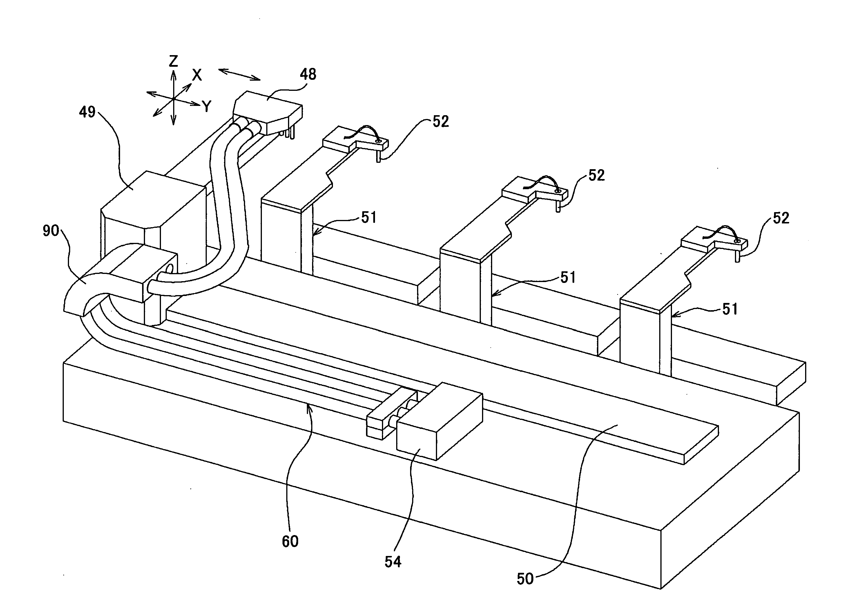
[0043]A description will be given below, with reference to the drawings, of embodiments according to the present invention. In the embodiments explained below, a complex pipe according to the present invention is applied to a resist coating / development processing apparatus of a semiconductor wafer.

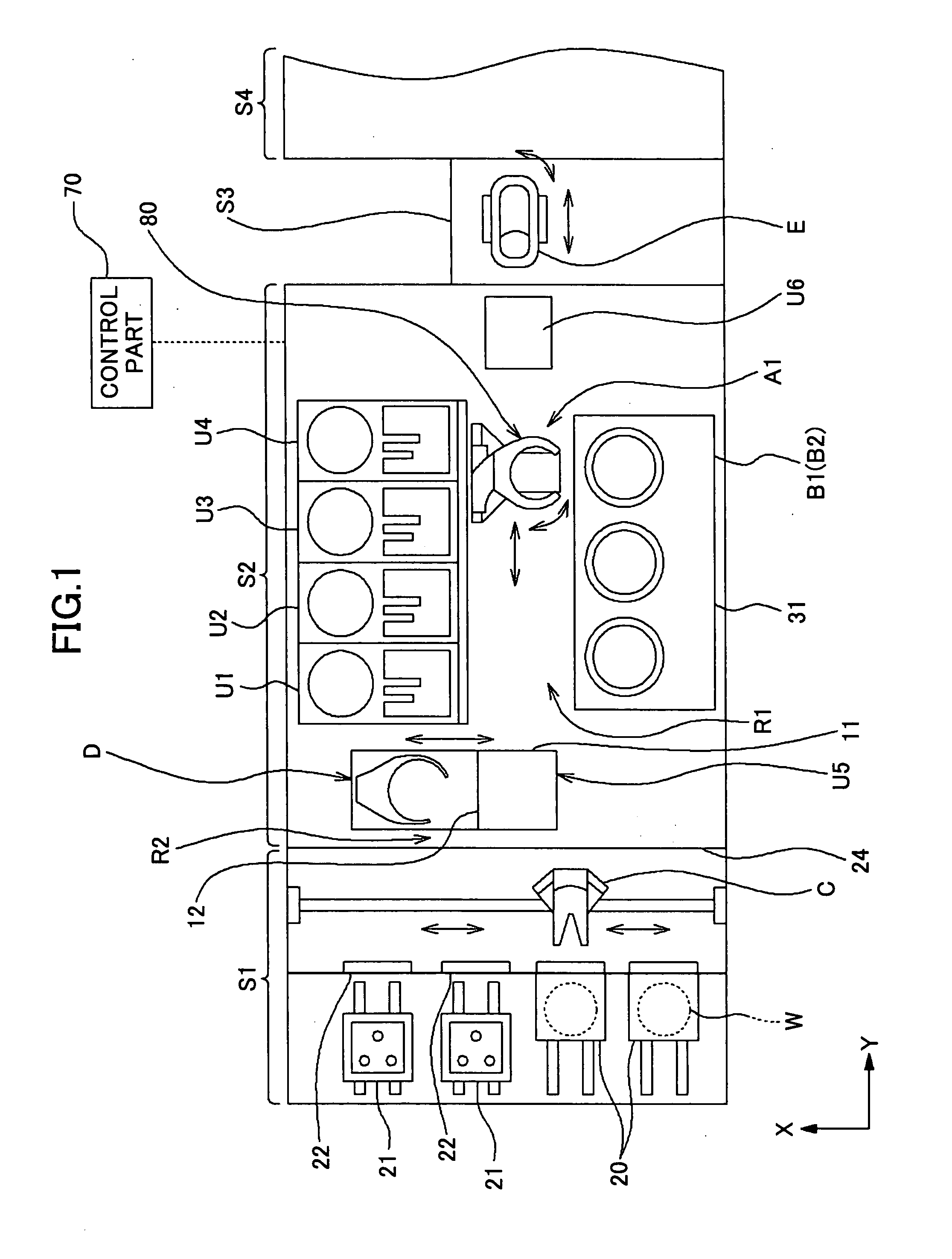
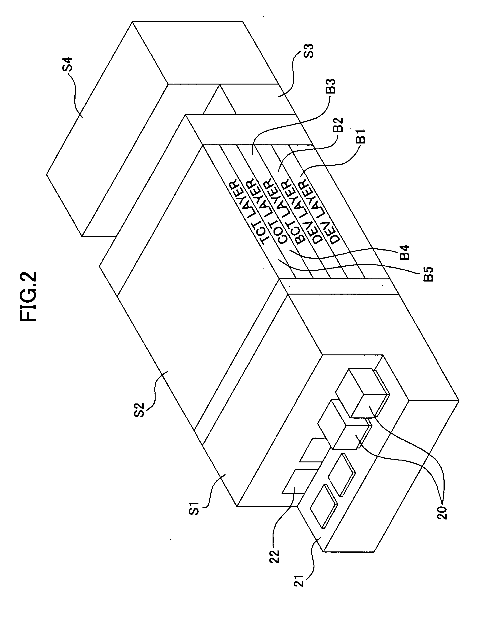
[0044]FIG. 1 is an outline plan view showing an example of a resist coating / development processing apparatus. FIG. 2 is an outline perspective view of the resist coating / development processing apparatus. FIG. 3 is an outline side view of the resist coating / development processing apparatus.

[0045]The resist coating / development processing apparatus comprises a carrier block S1 for conveying in and out a carrier 20 in which, for example, twenty-five sheets of semiconductor wafer W (hereinafter, referred to as wafer W), which is a substrate, are accommodated, a process block S2 constituted by arranging, for example, five unit blocks B1 to B5, an interface block S3 and an exposure apparatus S4.

[...


PUM


Abstract

In a complex pipe, a plurality of pipe members containing at least a pipe member for liquid and a pipe member for electricity are fixed in parallel arrangement. One end of the complex pipe is connected to a stationary equipment and the other end is connected to a movable member. The plurality of pipe members are integrally combined by a cover member having flexibility. A liquid supply pipe is inserted with a space in the pipe member for liquid. A fluid for temperature adjustment is supplied to the space between the pipe member for liquid and the liquid supply pipe.

Description

BACKGROUND OF THE INVENTION[0001]1. Field of the Invention[0002]The present invention relates to a complex pipe and a coating / development processing apparatus equipped with a complex pipe.[0003]2. Description of the Related Art[0004]Generally, in manufacture of semiconductor devices, in order to form a thin film or an electrode pattern of ITO (Indium Tin Oxide) on a substrate, such as a semiconductor wafer or an LCD glass substrate, a photo lithography technology is used. According to the photo lithography technology, a series of processes are performed including a process of forming a desired circuit pattern in a resist film by applying a photo resist onto a substrate, exposing the thus-formed resist film in accordance with a predetermined circuit pattern and development-processing the exposure pattern.[0005]Generally, such a process is performed by a coating / development processing apparatus equipped with a plurality of units such as a resist coating process unit, which applies a r...

Claims


Application Information

Patent Timeline
IPC IPC(8): F16L9/18F16L3/00B05C5/00
CPCH01L21/6715
Inventor NAKASHIMA, TSUNENAGAKISHITA, NAOFUMIHAYASHI, SHINICHI
Owner TOKYO ELECTRON LTD
Why Eureka
Try Eureka