

Analog-digital converter and image sensor
an analog-digital converter and image sensor technology, applied in the field of analog-digital converters and image sensors, can solve the problems of low conversion speed achievable by the integration-type ad converter, difficulty in sufficiently increasing the speed of ad conversion, and inability to appropriately perform ad conversion on the boundary between the upper bit and the lower bit, so as to reduce power consumption in operation, increase the accuracy, and reduce variation
- Summary
- Abstract
- Description
- Claims
- Application Information
AI Technical Summary
Benefits of technology
Problems solved by technology
Method used
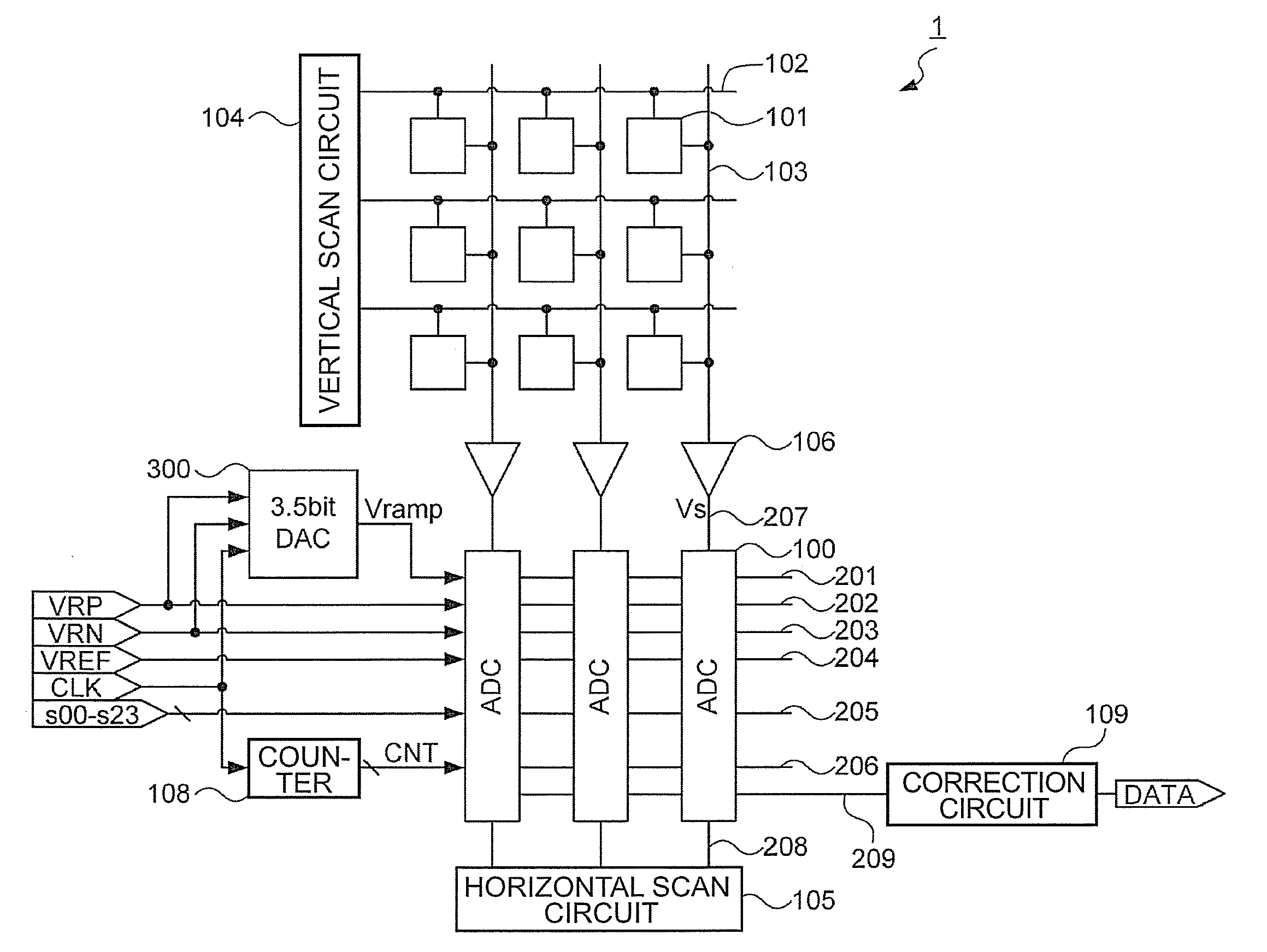
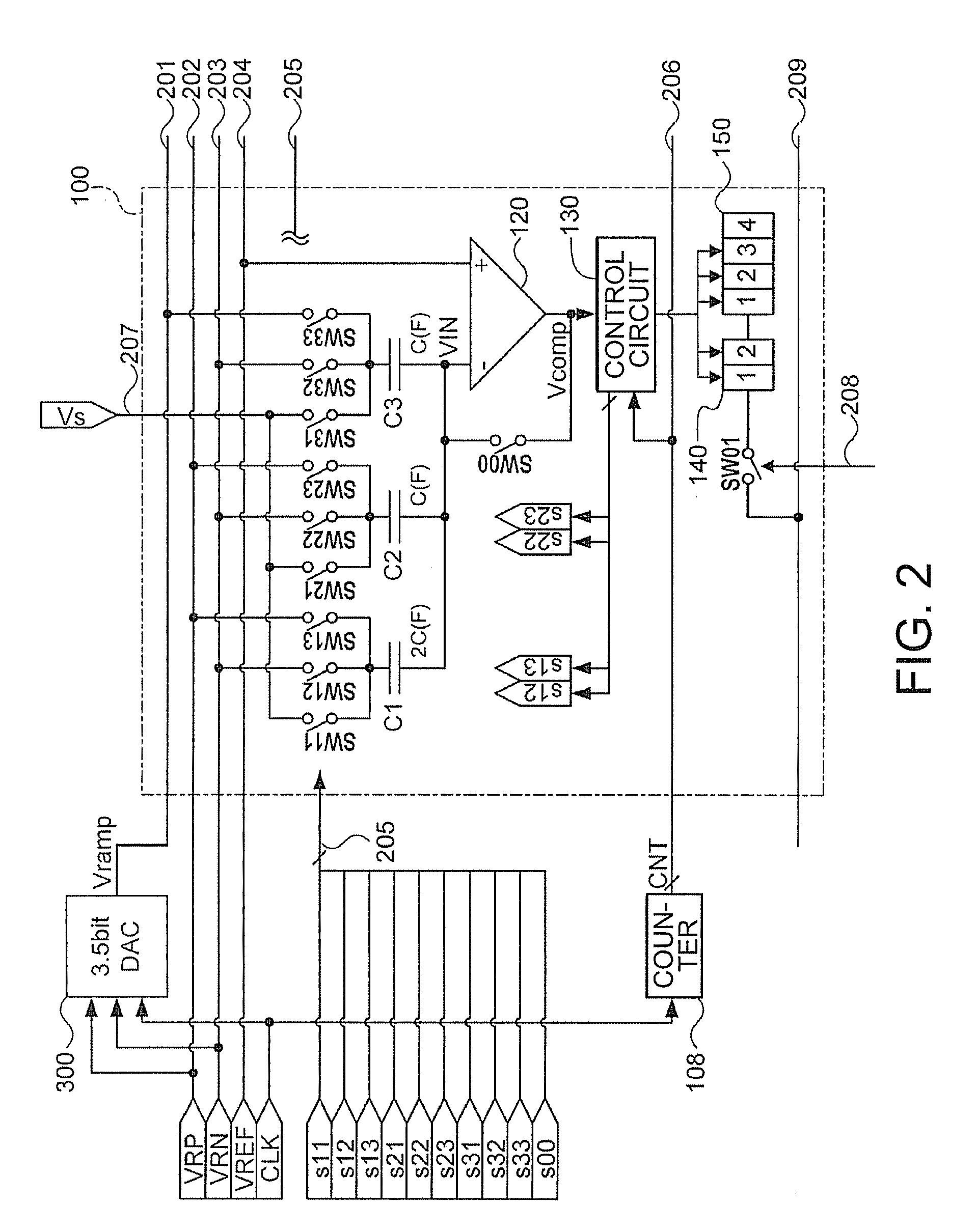
Image

Examples
modified example 1
[0077]An image sensor in a modified example 1 according to the invention is now discussed. In the embodiment, the upper two bits and the lower 3.5 bits of the analog signal Vs are converted into digital data. However, in case of conversion of upper 3 bits and lower 5 bits into digital data, for example, the first capacitor is set at 23−1CpF=4CpF, the second capacitor at 23−2CpF=2CpF, and the third capacitor at 23−3CpF=CpF. In this case, 5.5-bit DAC is employed in place of the 3.5-bit DAC 300, and 3-bit and 6-bit latch circuits are used.
modified example 2
[0078]An image sensor in a modified example 2 according to the invention is now described. While the structure shown in the embodiment has been applied to the image sensor, this structure may be applied to AD conversion using a number of converters disposed in a column such as a line sensor.
modified example 3
[0079]An image sensor in a modified example 3 according to the invention is now discussed. While the ramp voltage Vramp having 12 steps generated by the 3.5-bit DAC 300 is used in the embodiment, the number of the clock signals maybe decreased to 10 when preferable integration type AD conversion can be performed by ramp voltage Vramp having 10 steps.
PUM
 Abstract
Description
Claims
Application Information