High fidelity multiple resist patterning

a multi-resist patterning and high-fidelity technology, applied in the field of integrated circuit (ic) fabrication, can solve the problems of affecting the manner in which light is exposed, the circuit dimensions and device features continue to shrink, and the optical effect is adversely affected

Inactive Publication Date: 2008-11-27
GLOBALFOUNDRIES INC
View PDF5 Cites 108 Cited by
  • Summary
  • Abstract
  • Description
  • Claims
  • Application Information

AI Technical Summary

Benefits of technology

[0008]One embodiment may be carried out by a method of creating accurate photoresist features on a semiconductor wafer. The method involves: creating a first pattern of photoresist features over a target material of the semiconductor wafer; forming a second photoresist layer over the target material and over the first pattern of photoresist features, t

Problems solved by technology

This desire for large scale integration has led to a continued shrinking of circuit dimensions and device features.
This non-planar characteristic creates lensing and/or other optical effects that can adversely impact the manner in which light exposes the second photoresist layer during pattern exposure.
For example, the exposing light can be refracted or reflected in unpredictable ways that might alter the intended pattern, or the limited focal length of the lithograph

Method used


Image

  • High fidelity multiple resist patterning
  • High fidelity multiple resist patterning
  • High fidelity multiple resist patterning

Examples


Embodiment Construction

[0016]The following detailed description is merely illustrative in nature and is not intended to limit the embodiments of the invention or the application and uses of such embodiments. For the sake of brevity, conventional techniques and technologies related to photolithography, photoresist material composition, and semiconductor device fabrication may not be described in detail herein.

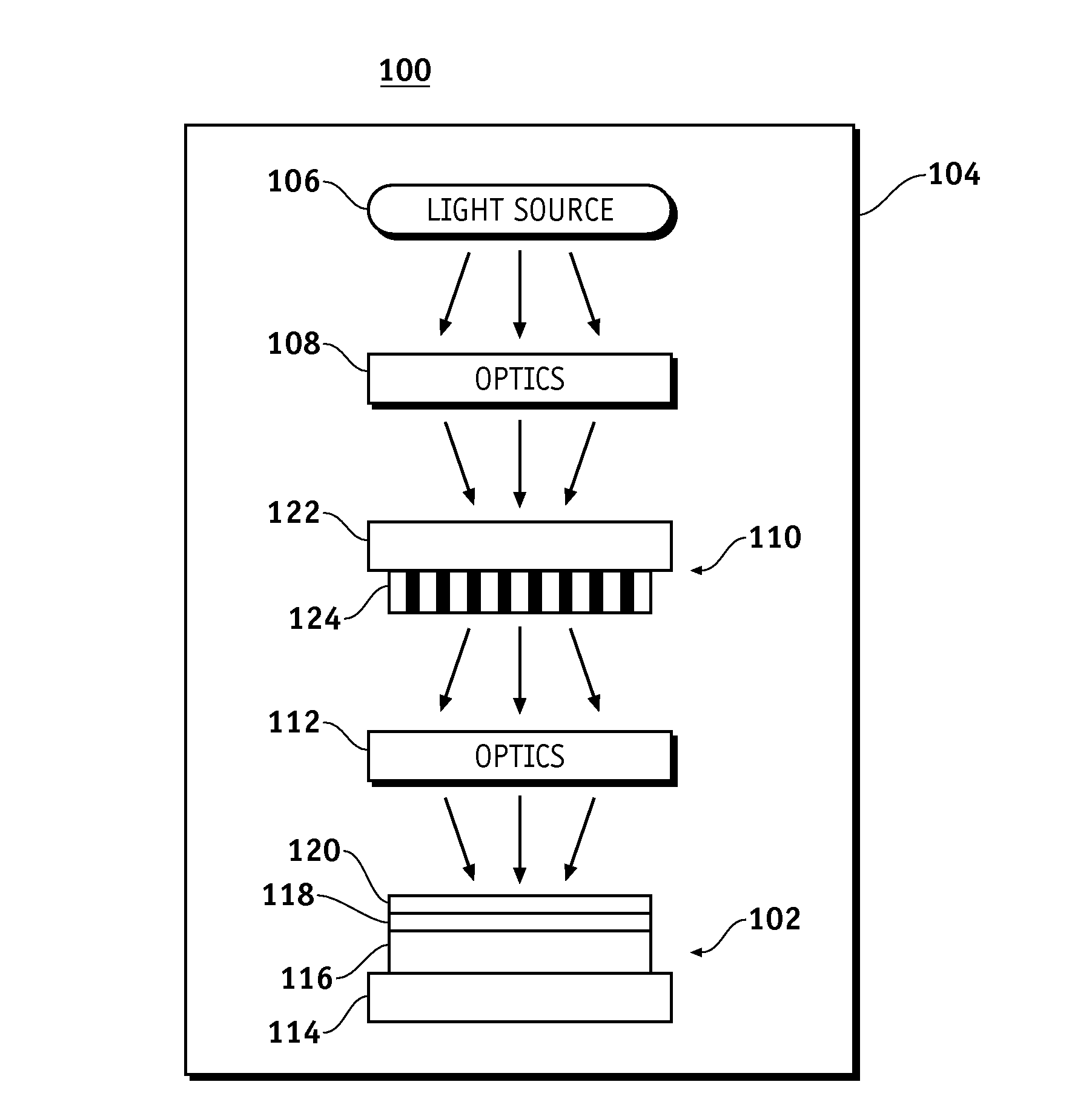
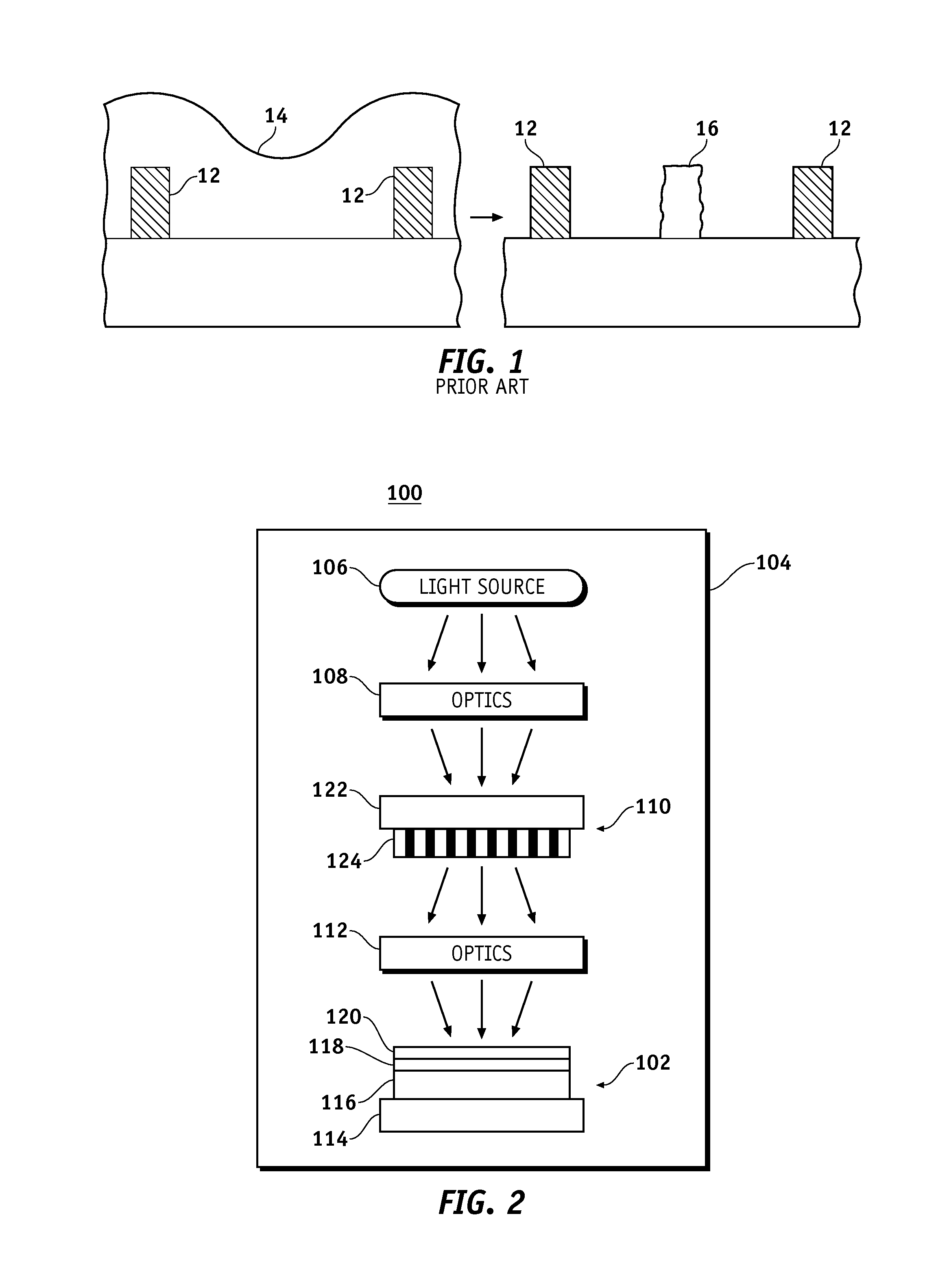
[0017]FIG. 2 is a schematic representation of a lithographic system 100 for patterning a wafer 102. Lithographic system 100 includes a chamber 104, a radiation source 106, a condenser lens assembly 108 (labeled “Optics” in FIG. 1), a mask or a reticle 110, an objective lens assembly 112 (labeled “Optics” in FIG. 1), and a stage 114. Lithographic system 100 is configured to transfer a pattern or image provided on mask or reticle 110 to a target material or surface of wafer 102. Lithographic system 100 may be a lithographic camera or stepper unit. For example, lithographic system 100 may be an XT1400 se...


PUM


Abstract

An integrated circuit fabrication process as described herein employs a double photoresist exposure technique. After creation of a first pattern of photoresist features on a wafer, a second photoresist layer is formed over the first pattern of photoresist features. The second photoresist layer is subjected to a reflow step that softens and relaxes the second photoresist material. This reflow step causes the exposed surface of the second photoresist layer to become substantially planar. Thereafter, the second photoresist layer can be exposed and developed to create a second pattern of photoresist features on the wafer. The planar surface of the second photoresist layer, which results from the reflow step, facilitates the creation of accurate, precise, and “high fidelity” photoresist features from the second photoresist material.

Description

TECHNICAL FIELD[0001]Embodiments of the disclosed subject matter relate generally to integrated circuit (IC) fabrication. More particularly, the embodiments relate to a technique for improving the quality of photoresist patterns associated with multiple-patterning IC wafer fabrication processes.BACKGROUND[0002]The semiconductor or IC industry aims to manufacture ICs with higher and higher densities of devices on a smaller chip area to achieve greater functionality and to reduce manufacturing costs. This desire for large scale integration has led to a continued shrinking of circuit dimensions and device features. The ability to reduce the size of structures, such as gate lengths in field-effect transistors and the width of conductive lines, is driven by lithographic performance.[0003]With conventional lithography systems, radiation is provided through or reflected off a mask or reticle to form an image on a semiconductor wafer. Generally, the image is focused on the wafer to expose a...

Claims


Application Information

Patent Timeline
IPC IPC(8): G03C5/00H01L21/31
CPCG03F7/0035G03F7/168H01L21/0273H01L21/3086
Inventor WALLOW, THOMAS I.KIM, RYOUNG-HANKYE, JONGWOOK
Owner GLOBALFOUNDRIES INC
Why Eureka
Try Eureka