Semiconductor substrate with electromagnetic-wave-scribed nicks, semiconductor light-emitting device with such semiconductor substrate and manufacture thereof

Active Publication Date: 2008-12-04
EPISTAR CORP
View PDF36 Cites 5 Cited by
  • Summary
  • Abstract
  • Description
  • Claims
  • Application Information

AI Technical Summary

Benefits of technology

[0012]Compared to the prior art, the substrate according to the invention is scribed by the electromagnetic wave to form a surface morphology such that light emitted from the semiconductor light-emitting device is scattered to reduce total reflection. Further, the external quantum efficiency and light-extraction efficiency of the semiconductor light-emitting device are enhanced. In particular, a conventional photolithography process is not required (i.e. mask-free) in the process of forming the surface morphology. Therefore, it takes much less time and reduces cost in the process of fabricating the substrate according to the invention.

Problems solved by technology

If a total reflection occurred when light is to be emitted out from the semiconductor light-emitting device, light would be reflected repeatedly until being absorbed in the interior of the device, which decreases the external quantum efficiency of the semiconductor light-emitting device.
These processes not only consume much time but cost much.

Method used


Image

  • Semiconductor substrate with electromagnetic-wave-scribed nicks, semiconductor light-emitting device with such semiconductor substrate and manufacture thereof
  • Semiconductor substrate with electromagnetic-wave-scribed nicks, semiconductor light-emitting device with such semiconductor substrate and manufacture thereof
  • Semiconductor substrate with electromagnetic-wave-scribed nicks, semiconductor light-emitting device with such semiconductor substrate and manufacture thereof

Examples


Embodiment Construction

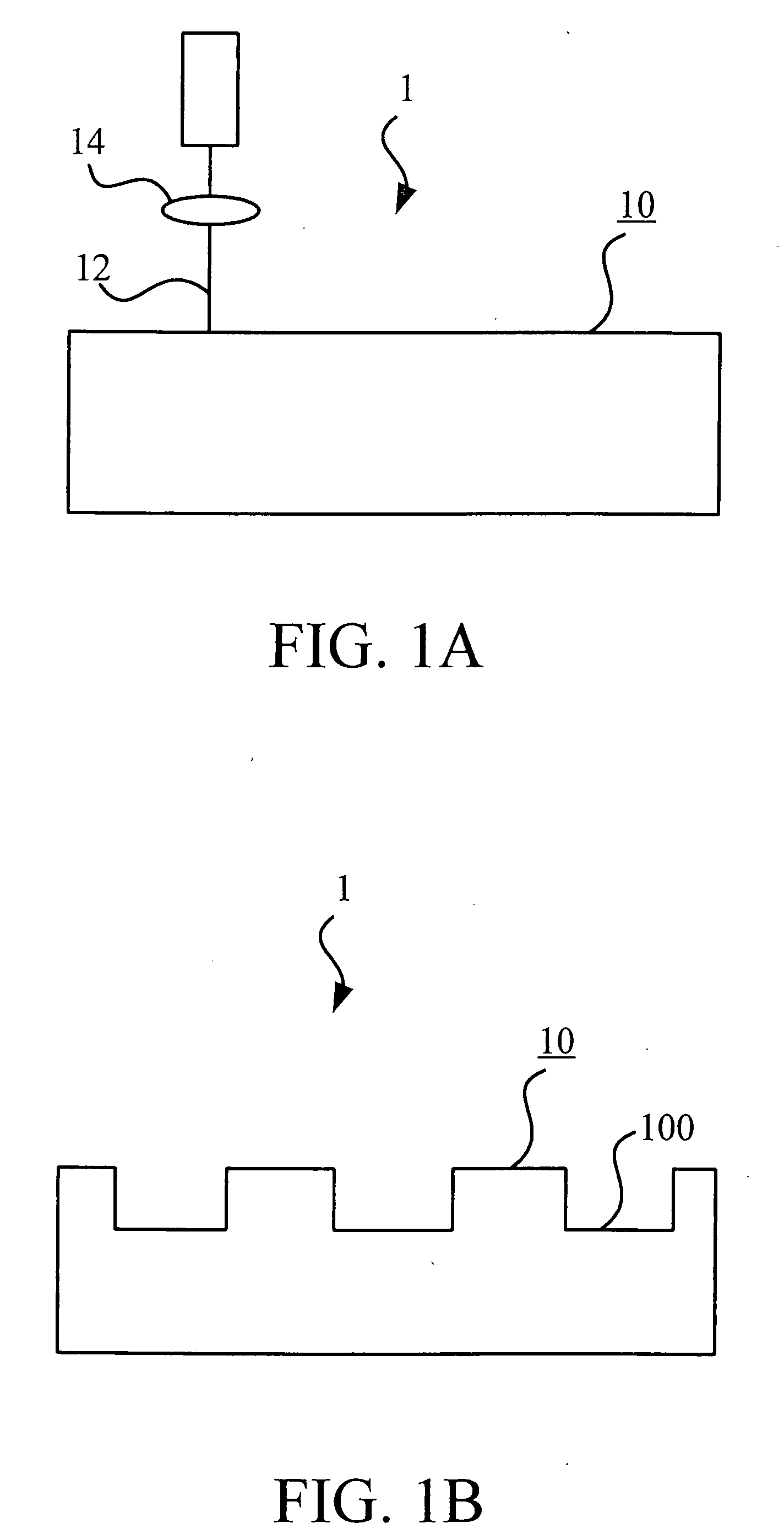
[0020]Please refer to FIG. 1A and FIG. 1B. FIG. 1A and FIG. 1B are the schematic diagrams of forming a substrate 1 according to an embodiment of the invention. The substrate 1 can be for epitaxy of a semiconductor light-emitting device.

[0021]In practical applications, the substrate 1 can be Si, GaN, AlN, sapphire, spinnel, SiC, GaAs, Al2O3, LiGaO2, LiAlO2, MgAl2O4.

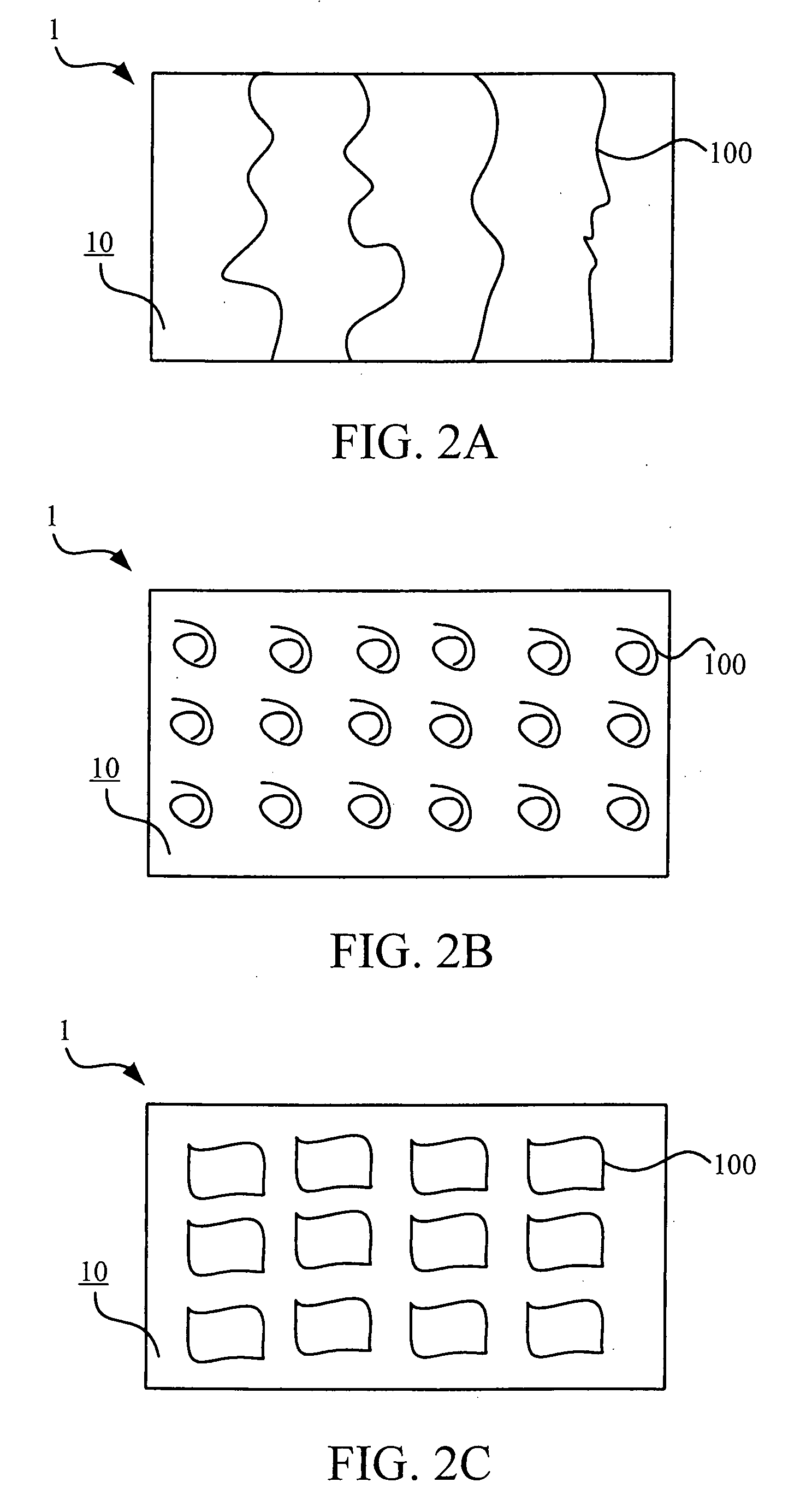
[0022]An upper surface 10 of the substrate 1 has a plurality of electromagnetic-wave-scribed nicks 100. The epitaxy of the semiconductor light-emitting device is to be performed on the upper surface 10 of the substrate 1. In practical applications, the electromagnetic wave can be visible light, micro-wave, infrared, ultraviolet, laser or other energy sources capable of forming the nicks 100 on the upper surface 10 of the substrate 1.

[0023]As shown in FIG. 1A, in one embodiment, the electromagnetic wave can be a laser beam 12. Thereby, the upper surface 10 of the substrate 1 can be scribed by the laser beam 12 to form the p...


PUM


Abstract

The invention discloses a substrate and a fabricating method thereof for epitaxy of a semiconductor light-emitting device. An upper surface of the substrate according to the invention, where the epitaxy of the semiconductor light-emitting device is to be performed, has a plurality of electromagnetic-wave-scribed nicks.

Description

BACKGROUND OF THE INVENTION[0001]1. Field of the Invention[0002]The present invention relates to a substrate and, more particularly, to a substrate for increasing the light-extraction efficiency of a semiconductor light-emitting device.[0003]2. Description of the Prior Art[0004]The current semiconductor light-emitting devices, such as light-emitting diodes, have been used for a wide variety of applications, e.g. illumination, remote control. To ensure high functional reliability as great as possible and a low power requirement of the semiconductor light-emitting devices, the external quantum efficiency is required for the devices.[0005]In principle, the external quantum efficiency of a semiconductor light-emitting device is determined both by the internal quantum efficiency and extraction efficiency. The internal quantum efficiency is determined by the material property and quality. The extraction efficiency refers to the proportion of radiation emitted from the interior of the devi...

Claims


Application Information

Patent Timeline
IPC IPC(8): H01L33/00H01L21/302H01L29/06H01L33/22
CPCH01L33/22H01L21/3043H01L29/30
Inventor TSAI, CHIUNG-CHITSAI, TZONG-LIANG
Owner EPISTAR CORP
Why Eureka
Try Eureka