Enhanced Output Impedance Compensation

Active Publication Date: 2008-12-04
AVAGO TECH INT SALES PTE LTD
View PDF43 Cites 6 Cited by
  • Summary
  • Abstract
  • Description
  • Claims
  • Application Information

AI Technical Summary

Benefits of technology

[0005]The present invention meets the above-noted need by providing, in an illustrative embodiment thereof, an enhanced compensation circuit operative to precisely control the output impedance of one or more metal-oxide-semiconductor (MOS) devices to be compensated over variations in PVT conditions to which the one or more MOS devices are subjected. To accomplish this, embodiments of the invention beneficially maintain a substantially constant drain-source voltage across one or more reference MOS devices substantially matched to one or more corresponding MOS devices to be compensated during a calibration cycle of the compensation circuit.

Problems solved by technology

However, such designs occupy significant silicon area, especially at low values of target output impedance due, at least in part, to electromigration and / or heat dissipation considerations.
Such conventional designs are therefore undesirable.

Method used


Image

  • Enhanced Output Impedance Compensation
  • Enhanced Output Impedance Compensation
  • Enhanced Output Impedance Compensation

Examples


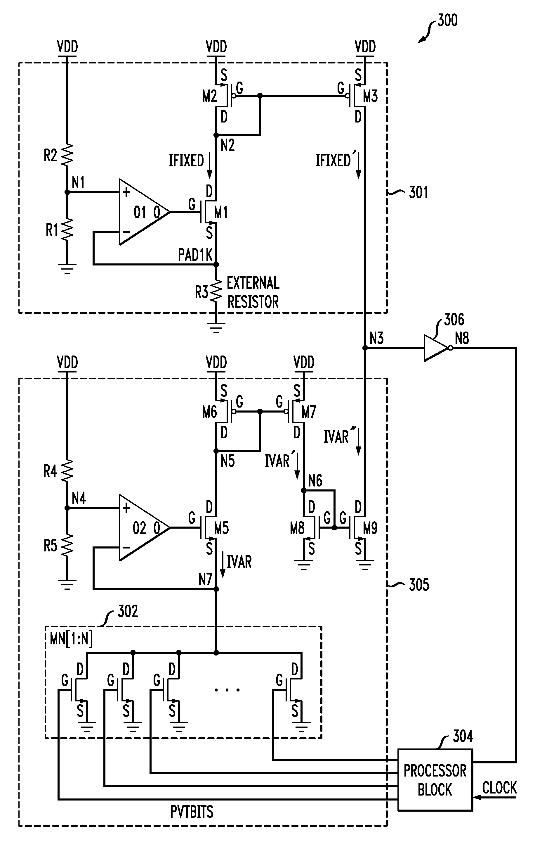
Embodiment Construction

[0012]The present invention will be described herein in the context of illustrative compensation circuits adapted to compensate for variations in output impedance due, at least in part, to variations in process, supply voltage and / or temperature (PVT) characteristics of an integrated circuit (IC). It should be understood, however, that the present invention is not limited to these or any other particular circuit arrangements. Rather, the invention is more generally applicable to techniques for reducing the chip area of a bidirectional buffer circuit. To accomplish this, embodiments of the invention utilize a multiplexing arrangement whereby two or more control signals supplied to the bidirectional buffer circuit share a single voltage level translator circuit, thereby reducing the number of voltage level translators required by the buffer circuit.

[0013]Although implementations of the present invention are described herein with specific reference to p-channel metal-oxide-semiconducto...


PUM


Abstract

A compensation circuit for compensating an output impedance of at least a first MOS device over PVT variations to which the first MOS device may be subjected includes a first current source generating a first current having a value which is substantially constant and a second current source generating a second current having a value which is programmable as a function of at least one control signal presented to the second current source. A comparator is connected to respective outputs of the first and second current sources and is operative to measure a difference between the respective values of the first and second currents and to generate an output signal indicative of relative magnitudes of the first current and the second current. A processor connected in a feedback arrangement between the comparator and the second current source receives the output signal generated by the comparator and generates the control signal for controlling the second current as a function of the output signal. The processor is operative to control the value of the second current so that the second current is substantially equal to the first current.

Description

FIELD OF THE INVENTION [0001]The present invention relates generally to electronic circuits, and more particularly relates to output impedance compensation techniques in a circuit.BACKGROUND OF THE INVENTION [0002]In modern electronic circuits, such as, for example, input / output (IO) buffers, it is desirable to control the output impedance of the IO buffers for a variety of reasons, including, but not limited to, transmission line matching, minimizing switching noise (di / dt), optimizing signal swing, etc. Various IO standards, such as, for example, stub series terminated logic (SSTL), high-speed transceiver logic (HSTL), etc., specify the output impedance and / or output current of a receiver at specific values of output voltage (e.g., Vol or Voh) in order to ensure that there is sufficient margin for the receiver to function properly. While most IO standards specify an upper limit for output impedance (or a lower limit for output current), switching noise and / or transmission line mat...

Claims


Application Information

Patent Timeline
IPC IPC(8): G06G7/12
CPCH03K19/00384H04L5/16H04L25/0264
Inventor BHATTACHARYA, DIPANKARKOTHANDARAMAN, MAKESHWARKRIZ, JOHN C.MARQUES, ANTONIO M.MORRIS, BERNARD L.
Owner AVAGO TECH INT SALES PTE LTD
Why Eureka
Try Eureka