Camera module package and method of manufacturing the same

Inactive Publication Date: 2008-12-11
SAMSUNG ELECTRO MECHANICS CO LTD
View PDF5 Cites 27 Cited by
  • Summary
  • Abstract
  • Description
  • Claims
  • Application Information

AI Technical Summary

Benefits of technology

[0027]The advantages of the present invention are achieved by providing a camera module package including a silicon wafer mounted with the image sensor in a center of a top surface thereof and provided with pads both sides of the image sensor, a lens unit opened to form a convex lens in a mounting portion of the image sensor in an upper part of the wafer, and a flexible board tightly joined to a bottom surface of the wafer and electrically connected to the pads by an internal pattern.
[0028]An IR filter layer for selectively shielding ultraviolet rays included in incident light is further formed on a top surface of the lens formed in the center of the lens unit.
[0029]A

Problems solved by technology

Accordingly, the camera module manufactured in the above-mentioned method has a limit in decrement in a size and decrement in a thickness and has the low flexibility of a shape change since all the camera modules are configured in a rigid material a

Method used


Image

  • Camera module package and method of manufacturing the same
  • Camera module package and method of manufacturing the same
  • Camera module package and method of manufacturing the same

Examples


first embodiment

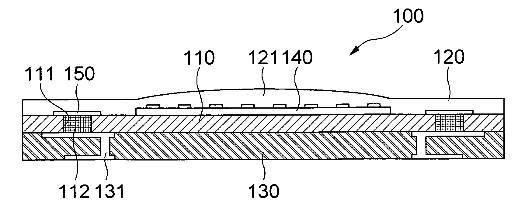
[0102]FIGS. 18A to 18E are flowcharts in which a lens unit is formed by the laminating method using the monolayer film sheet adopted in the invention. As shown in the figure, a film sheet 120a made of a polymer used at the time of manufacturing the lens is adhered onto the top surface of the wafer 110 including the top surface of the image sensor 140 by using a laminator apparatus (see FIG. 18B).

[0103]At this time, the film sheet 120a is preferably made of a photosensitive material.

[0104]Next, a pattern 120a′ is formed on the film sheet 120a by a photolithography process, that is, processes such as an exposure, a development, and the like (see FIG. 18C) and the lens 121 is formed as a formation part of the pattern 120a is softened by performing a reflow process in a state that the pattern 120a′ is formed on the film sheet 120a (see FIG. 18D).

[0105]After then, the individual camera module packages are manufactured as the wafer 110 is diced along the scribe line 180 formed between the...

second embodiment

[0106]FIGS. 19A to 19F are flowcharts in which the lens unit is formed by the laminating method using the multilayer film sheet adopted in the invention. As shown in the figure, a first film sheet 120a is adhered onto the top surface of the wafer 110 including the top surface of the image sensor 140 by using the laminator apparatus (see FIG. 19B).

[0107]The top surface of the first film sheet 120a is thinned by the exposure, the development, or the thinning process. A second film sheet 120b is laminated on the top surface of the first film sheet 120a (see FIG. 19C).

[0108]The second film sheet 120b is made of a photosensitive material and a pattern 120b′ is formed on the second film sheet 120b through the photolithography process, that the processes such as the exposure, the development, and the like (see FIG. 19D).

[0109]Herein, a principal object to adhere the first film sheet 120a first is to strength adhesion force between the second film sheet 120b to be applied hereafter and the ...

third embodiment

[0113]FIGS. 20A to 20E are flowcharts in which the lens unit is formed by the laminating method using the film sheet having the pattern adopted in the invention. As shown in the figure, the first film sheet 120a is adhered onto the top surface of the wafer 110 including the top surface of the image sensor 140 by using the laminator apparatus (see FIG. 20B).

[0114]The top surface of the first film sheet 120a is thinned by the exposure, the development, or the thinning process. The second film sheet 120b having patterns arranged with equal spacing is laminated on the top surface of the first film sheet 120a (see FIG. 20C).

[0115]Since the lens 121 may be formed without the process such as the exposure or the development, the second film sheet 120b needs not to be made of the photosensitive material. The photolithography process for forming the lens pattern 121b′ described in the above-mentioned embodiments may be omitted.

[0116]Herein, the principal object to adhere the first film sheet ...


PUM


Abstract

The present invention relates to a camera module package having flexibility and a method of manufacturing the same. Provided is the camera module package according to the invention including a silicon wafer mounted with the image sensor in the center of a top surface thereof and provided with pads both sides of the image sensor, a lens unit opened to form a convex lens in a mounting portion of the image sensor in an upper part of the wafer, and a flexible board tightly joined to a bottom surface of the wafer and electrically connected to the pads by an internal pattern. The camera module package can be thinly manufactured and since the camera module package has flexibility, the camera module package can be easily attached to a bendable substrate and to the inside an IT apparatus.

Description

CROSS-REFERENCE TO RELATED APPLICATIONS[0001]This application claims the benefit of Korean Patent Application No. 10-2007-0055153 filed with the Korea Intellectual Property Office on Jun. 5, 2007, the disclosure of which is incorporated herein by reference.BACKGROUND OF THE INVENTION[0002]1. Field of the Invention[0003]The present invention relates to a camera module package having flexibility and a method of manufacturing the same and, more particularly, to a camera module package which has the flexibility and can be thinly manufactured by sequentially stacking a silicon board mounted with an image sensor on a top surface of a flexible board and a lens unit in a wafer level state.[0004]2. Description of the Related Art[0005]In recent years, camera modules are mounted on IT apparatuses including a mobile communication terminal, a PDA (Personal Digital Assistant), and an MP3 player, an automobile, an endoscope, and the like at the time of manufacturing the IT apparatuses, the automob...

Claims


Application Information

Patent Timeline
IPC IPC(8): G03B17/00H01L21/00G02B7/02H04N5/335H04N5/369
CPCH01L27/14618H01L27/14627H01L27/14683H04N5/2253H04N5/2254H04N5/2257H01L2224/48091H04N23/54H04N23/57H04N23/55H01L2924/00014H01L27/14H04N23/00
Inventor JEUNG, WON KYUCHOI, SEOG MOONYUAN, JINGLILIM, CHANG HYUNKIM, DAE JUN
Owner SAMSUNG ELECTRO MECHANICS CO LTD
Why Eureka
Try Eureka